ALLPCB


1 Structure Overview
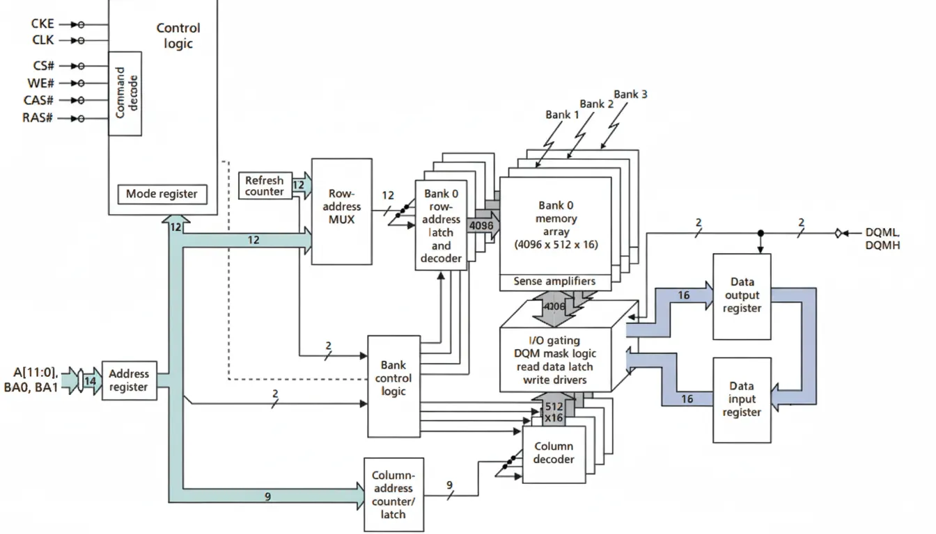
This article continues an analysis of internal block diagrams, focusing on DDR, DDR2, and DDR3 memory chips to identify their differences. The following figure shows a Micron 128Mb SDRAM chip block diagram; the previous article covered that diagram in detail.
To increase memory read/write bandwidth, SDRAM originally relied on raising the clock frequency. Due to limitations such as temperature, SDRAM core clock frequency is constrained. SDRAM transmits data only on the rising clock edge. DDR increases data transfer rate by transmitting data on both the rising and falling edges of the I/O clock, while the internal core still transfers data only on the rising edge. To match the core (single-edge) and the I/O port (double-edge) transfer rates, the core data bus width is doubled relative to the I/O data bus width, i.e., 2n prefetch. This is the basic DDR design principle.
The images below show the internal block diagram of a Micron DDR chip, model MT46V32M16P-6T. Like the SDRAM example, this chip has a 16-bit data bus and 512Mb capacity. Ignoring capacity, the key difference is the red-highlighted area: DDR uses a differential clock.

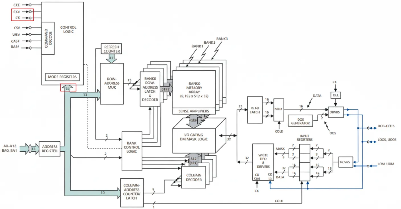
During a write, the receiver registers capture incoming DQ[0:15] data and the data mask signals (LDM/UDM). These input registers function similarly to IDDR: they convert 16-bit data transferred on both edges of DQS into 32-bit data on a single edge. The 2-bit DM signals are converted into 4-bit MASK signals. The resulting 32-bit single-edge data and 4-bit MASK are sent to a write FIFO. The write FIFO handles the asynchronous clock domain crossing, synchronizing DATA and MASK from the DQS domain to the internal core clock CK so data can be written into the internal array with correct timing.
Note that both the input registers and the write FIFO sample data using DQS as the capture clock because the DQS edges are center-aligned with the write data DQ and the mask DM.
Some readers may ask: DQ is transferred on both edges of CK, so why sample DQ using DQS? DQS is the data strobe. On reads, DQS edges align with DQ edges; on writes, DQS edges align with the center of DQ. Therefore sampling on DQS edges during write provides more stable data sampling.
On a read, the bank transfers 32-bit data to a read latch under the internal clock. The 32-bit word is split into two 16-bit values, selected by a MUX, and then driven onto the external bus under control of the DQS generator. The DQS generator times the transfers so the 16-bit halves are sent on the rising and falling edges of the external clock.
If the external clock is 100 MHz, the I/O transfers occur on both edges, yielding a 200 MT/s data rate. This illustrates the DDR working principle: internal storage width = 2 × I/O width, the so-called 2-bit prefetch (or 2n prefetch, where n is the chip I/O width).
Another difference in the block diagrams: SDRAM uses 12 address lines as mode register data signals, while DDR shows 15 lines connected to the mode registers: 13 address lines and 2 bank address lines. DDR adds an extended mode register (EMR) in addition to the mode register (MR). During configuration, the bank address lines select whether A12~A0 are interpreted as MR or EMR data.
2 Functional and Structural Differences
DDR SDRAM and SDRAM share many commands and functions, such as ACT (activate) and auto precharge, so this section focuses on the differences.
2.1 Clock
SDRAM uses a single-ended clock signal, while DDR uses a differential clock pair. CK# helps correct timing between rising and falling edges. Because data is transferred on both edges of CK, the transfer period is halved and the timing between rising and falling edges must be precise. Variations caused by temperature or changes in line impedance can alter the spacing between edges; the complementary CK# signal helps compensate (if CK rises quickly and falls slowly, CK# will rise slowly and fall quickly).
Sampling at the CK/CK# cross point compensates for edge spacing variation. Since data uses both clock edges, CAS latency (CL) can be 1.5 or 2.5 cycles. Data and related signals are transferred on both edges, while command/address signals remain single-edge (rising edge) driven.
2.2 Mode Registers and Initialization
Like SDRAM, DDR requires mode register setup (MRS) at power-up. DDR adds an extended mode register set (EMRS) stage because additional operational controls are required, such as enabling/disabling DLL, output drive strength, and optional QFC.
The DDR mode register layout differs: burst length no longer supports full-page, and CL options change. To distinguish MR and EMR during configuration, BA1~BA0 are used: BA1~BA0 = 00 selects MR, BA1~BA0 = 01 selects EMR, with A[n:0] providing the register data.
The chip's EMR controls DLL enable/disable and QFC enable/disable, among other options. DLL will be explained later.
QFC refers to a FET Switch Controller (active low). It allows external FETs to isolate memory devices on a module when they are idle to prevent crosstalk between devices. QFC is an optional feature that manufacturers may add only on customer request and requires module-level design changes (for example, adding pull-up resistors on VddQ). QFC is rarely found in the market and is not defined in more recent JEDEC DDR specifications; the device manual may state it is unsupported.
Because DDR adds an extended mode register, the initialization sequence differs. After power is stable and a 200 μs delay, clocks are enabled, all banks are precharged, EMR and MR are programmed, banks are precharged again, and finally two auto-refresh cycles are issued before entering normal operation.
2.3 Burst Length and Write Mask
SDRAM supports burst lengths of 1, 2, 4, 8, and full-page. DDR supports burst lengths of 2, 4, and 8. Note: SDRAM burst length refers to the number of consecutive addressed storage locations; DDR burst length refers to the number of consecutive transferred data words, each word equal to the chip I/O width. Because DDR stores twice the I/O width per core access, the chip always transfers at least two data words, so a burst length of 1 does not exist. Full-page bursts were more useful in imaging applications but were removed for PC memory usage, which was the primary DDR application at the time.
For writes, DDR supports masking via DM signals similar to SDRAM. DM and DQ are issued together; the DDR chip samples DM on both edges of DQS. If DM is high, that corresponding DQ data is discarded and not written to internal memory.
SDRAM also has write mask for reads, but DDR read operations do not support mask functionality because the controller determines which data to read; unwanted data can simply be avoided by the controller.
2.4 Delay-Locked Loop (DLL)
The following explanation is based on a technical article. DDR requires high clock precision and uses two clocks: the external bus clock and the internal core clock. Ideally they are synchronized, but temperature and voltage variations make perfect sync difficult. SDRAM also has an internal clock, but synchronization issues are less severe due to lower operating frequency.
Clock misalignment can be positive or negative relative delay. A fixed offset (for example, one clock period) might keep rising and falling edges aligned conceptually, but because the external clock period can vary, DDR must dynamically adjust the internal clock delay to match the external clock. This function is performed by a delay-locked loop (DLL) which monitors and adjusts internal clock delay to maintain alignment with the external clock.
DLL does not change frequency or voltage; it produces a delay value for the internal clock. Two common DLL implementation methods are Clock Frequency Monitor (CFM) and Clock Comparison (CC).
CFM measures the external clock frequency and adjusts internal delay to ensure internal and external clocks differ by approximately one period. CFM can correct quickly, within two clock cycles, but is sensitive to noise and measurement error, which can lead to persistent misadjustments.
CC compares internal and external clock periods and adjusts the internal delay incrementally. If the internal clock period is shorter than the external clock, CC adds delay on the next internal cycle; if longer, it reduces delay. The process repeats until synchronization is reached. CC is more robust and stable, as errors affect only isolated data points and do not propagate, but CC converges more slowly than CFM.
DLL can be disabled during diagnosis and evaluation; in normal operation it is typically enabled and automatic. The DLL function is essentially to align the internal and external clocks by inserting or removing delay.
2.5 Data Strobe (DQS)
DDR adds the DQS strobe signal, which does not exist in SDRAM. There is one DQS per byte. For a 16-bit device, two bytes mean LDQS and UDQS. DQS helps identify each transfer within a clock cycle and enables the receiver to sample data accurately. DQS is bi-directional and is used to synchronize with DQ.
On reads, DQS and DQ are generated together (at the CK/CK# cross point). In DDR, CAS latency refers to the interval from the CAS command to DQS generation. The time between DQS triggering and the data appearing on the I/O is called tAC. Note that DDR tAC differs in meaning from SDRAM tAC.
When DQS is generated, internal prefetching is already complete; tAC refers to the data output time from the prefetch stage. Prefetching may cause data to be available slightly before DQS is asserted.
On writes, DQS edges are center-aligned with the DQ data, providing a stable sampling point so DDR devices can capture DQ on DQS edges.
2.6 Write Latency (tDQSS)
In SDRAM, the write command and write data appear on the bus simultaneously. In DDR, after issuing a write command there is a write latency tDQSS before DQS, write data DQ, and DM become valid. tDQSS is the delay from the write command to the first corresponding rising edge of DQS.
tDQSS ensures synchronization: with two transfers per clock cycle, timing precision is critical and receivers must be prepared before data transfer begins. tDQSS is an important DDR parameter: too short may cause capture errors, too long wastes bus time. tDQSS is typically between 0.75 and 1.25 clock cycles, usually approximately one clock cycle. Because DQS and CK may be unsynchronized, the DDR clock is mainly used to synchronize command timing. Data reads and writes themselves are synchronized to DQS, and a write FIFO transfers data from the DQS domain to the CK domain, so DQS/CK phase difference does not prevent correct data writes.
Because data is transferred on both edges while commands are single-edge, when CL=2.5 the next command after a read must be delayed by an extra half clock period. For example, when issuing a write after a read with CL=2.5, add half a clock to tDQSS.
DDR write completion requires additional internal processing steps, so write recovery time tWR is longer (typically around 3 clock cycles). In DDR2, tWR is exposed as a mode register parameter.
3 Conclusion
- DDR transfers data on both edges of the clock, delivering two I/O-width data words per clock. SDRAM transfers only on the rising edge, one I/O-width word per clock.
- To meet tighter timing requirements, DDR uses a differential clock and does not support clock suspend operations.
- Because the core transfers data only on a single edge, DDR uses a 2n prefetch: the internal data bus is twice the width of the I/O bus to convert double-edge I/O data to single-edge core data.
- DDR does not support single-beat or full-page burst transfers. Read operations do not support mask functionality.
- Because DDR uses double-edge transfers, CAS latency can be 2.5 cycles. SDRAM has no write command-to-data delay, while DDR requires tDQSS between the write command and the appearance of DQ, DM, and DQS.
- DDR introduces the DQS strobe. On reads DQS edges align with DQ edges; on writes DQS edges align with the center of DQ, enabling stable capture on DQS edges.
- DDR adds a delay-locked loop (DLL) to align internal and external clocks due to tighter clock precision requirements.
- SDRAM typically uses 3.3 V LVTTL signaling, while DDR uses 2.5 V SSTL_2 signaling, reducing DDR power. SDRAM commonly uses TSOP-II packages; DDR devices are available in TSOP-II and BGA packages.
This article is based on DDR and SDRAM documentation and technical analysis. After using IDDR primitives, converting double-edge transfers to single-edge transfers becomes straightforward, and read/write behavior is easier to analyze. FPGA designs typically use vendor DDR IP cores to handle DDR devices; however, when a custom carrier or memory board is used, understanding DDR behavior is essential to isolate issues between the FPGA and hardware. The next article will analyze how DDR evolves into DDR2.