ALLPCB


What Are Blind and Buried Vias and Why Optimization Matters
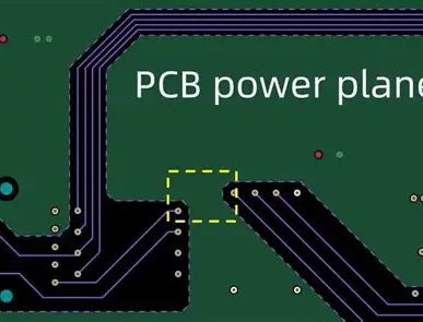
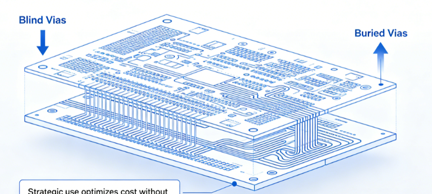
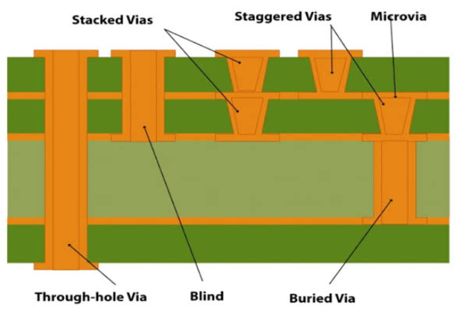
A blind via connects an outer layer to one or more inner layers without extending through the entire board thickness. A buried via, by contrast, links only inner layers and remains hidden from the outer surfaces. Both differ from conventional through vias that span all layers. In high-density interconnect constructions, these options support finer routing channels and smaller component footprints. Their adoption often ties directly to HDI PCB cost optimization efforts, as they can reduce the need for additional signal layers in complex layouts. Proper planning around these features helps control expenses while meeting electrical and mechanical requirements.
Industry relevance stems from the push toward smaller, more capable devices across sectors such as telecommunications and automotive electronics. Designers face pressure to deliver reliable boards at competitive prices. Blind and buried via usage influences material consumption, processing time, and yield rates. When overused or poorly placed, they can elevate expenses through extra fabrication steps. Strategic application, however, aligns with broader PCB cost reduction strategies by streamlining the overall build.
Technical Principles Behind Via Implementation and Associated Costs
Manufacturing blind and buried vias typically requires sequential lamination processes rather than a single drilling operation. Each additional via type may involve separate drilling, plating, and filling cycles that extend production timelines. Laser drilling often creates the small diameters needed for these features, adding precision equipment demands compared with mechanical methods. Alignment tolerances between layers become critical, as even minor shifts can lead to connectivity issues or scrap. These steps contribute to the primary blind via cost drivers and buried via cost drivers observed in fabrication.
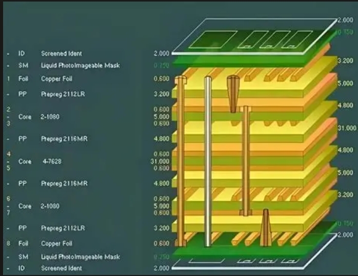
Layer stackup optimization plays a central role in managing these variables. Engineers evaluate dielectric thicknesses, copper weights, and via aspect ratios early in the design to determine feasible via placements. Higher aspect ratios can complicate plating uniformity and increase defect risks during thermal cycling. Standards such as IPC-6012 provide guidance on acceptable performance criteria for rigid boards, including via integrity under qualification testing. Careful modeling of the stackup helps identify opportunities to combine via types or limit their total number without sacrificing routing density.
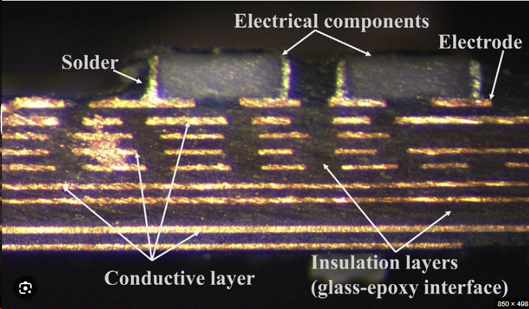
Thermal and mechanical stresses also factor into long-term reliability. Repeated lamination cycles for buried features can induce warpage or delamination if material selections and cure profiles are not matched properly. 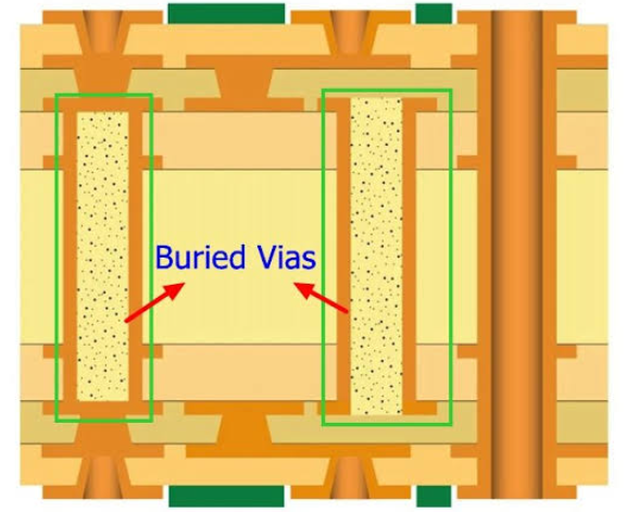 Designers review coefficient of thermal expansion values across the stack to maintain stability. These engineering considerations directly influence yield and therefore overall project economics in HDI constructions.
Practical Design Approaches for Cost Optimization
Effective layer stackup optimization begins with mapping all required connections and identifying which can use through vias instead of blind or buried options. Placing blind vias only at necessary outer-to-inner transitions reduces the number of sequential build-up stages. Similarly, grouping buried vias within fewer inner layer pairs limits the total lamination cycles required. Simulation tools allow verification of signal integrity and thermal performance before committing to a final configuration.
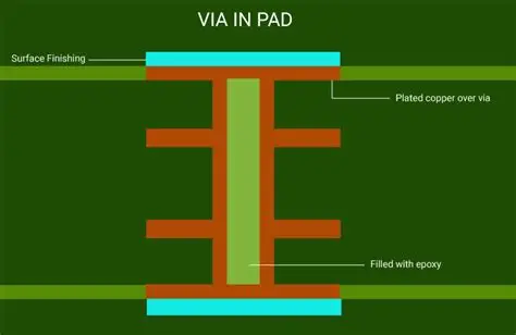
Design rules should incorporate manufacturing capabilities from the outset. Specifying via diameters and capture pad sizes compatible with standard processes avoids custom tooling charges. Engineers also consider via filling materials and planarization steps, which add cost when applied indiscriminately. Reviewing the board for opportunities to share vias across multiple nets or to route signals on fewer layers supports HDI PCB cost optimization goals.
Collaboration between design and fabrication teams helps surface potential issues early. For instance, confirming drill-to-copper clearances and registration tolerances prevents costly revisions later. Applying these practices consistently contributes to reliable outcomes while controlling the variables that drive expenses in blind and buried via implementations.
Conclusion
Optimizing blind and buried via usage requires balancing electrical performance needs against manufacturing realities. Thoughtful application of these features supports PCB cost reduction strategies when integrated into a well-planned layer stackup. Attention to process steps, alignment requirements, and material interactions helps limit the impact of blind via cost drivers and buried via cost drivers. Engineers who apply structured evaluation methods achieve more predictable results in HDI constructions. Ultimately, these approaches contribute to boards that meet both technical specifications and budgetary targets.
FAQs
Q1: What are the primary blind via cost drivers in multilayer PCB production?
A1: Blind via cost drivers include additional sequential lamination cycles, laser drilling operations, and tighter alignment requirements during fabrication. These factors increase processing time and can affect yield when not managed through careful design. Layer stackup optimization helps reduce unnecessary blind via counts while preserving routing capability.
Q2: How does layer stackup optimization influence buried via cost drivers?
A2: Layer stackup optimization allows designers to consolidate buried via locations within fewer inner layer pairs, thereby limiting the number of build-up stages. This approach reduces material handling and thermal stress accumulation during manufacturing. The result supports more economical HDI PCB cost optimization without compromising interconnect density.
Q3: Which PCB cost reduction strategies work best when incorporating blind and buried vias?
A3: Effective strategies focus on using through vias wherever possible, specifying standard via dimensions, and verifying stackup feasibility early with fabrication input. These steps minimize custom processes and improve overall yield. Consistent application of design rules aligned with industry expectations further aids cost control.
Q4: Why is via type selection important for HDI PCB cost optimization?
A4: Via type selection determines the complexity of the fabrication sequence and the total number of processing steps required. Blind and buried options enable compact layouts but introduce cost drivers when overapplied. Strategic choices based on electrical needs and manufacturing constraints deliver balanced outcomes.
References
IPC-6012E — Qualification and Performance Specification for Rigid Printed Boards. IPC, 2017
IPC-A-600K — Acceptability of Printed Boards. IPC, 2020
JEDEC J-STD-020E — Moisture/Reflow Sensitivity Classification. JEDEC, 2014