If you're new to printed circuit board (PCB) design and wondering about copper pour basics or how PCB grounding works, you're in the right place. In simple terms, a copper pour is a technique where unused areas of a PCB are filled with copper, often connected to ground, to improve electrical performance and reduce noise. Grounding, on the other hand, ensures a stable reference point for signals, preventing interference and enhancing safety. This blog offers an intro to copper pour, a copper fill tutorial, and a clear guide to simple PCB design practices. Let's dive deeper into these concepts with practical tips and easy-to-understand explanations.
What Is Copper Pour and Why Does It Matter in PCB Design?
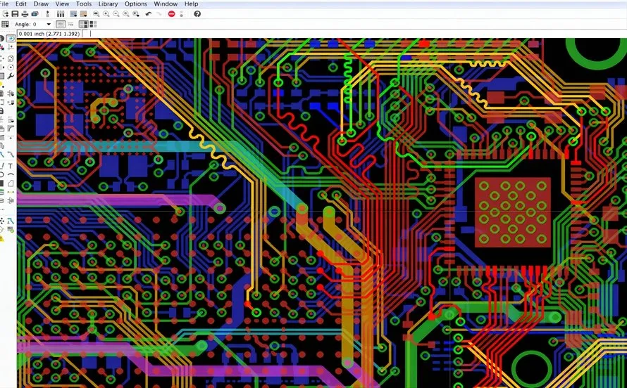
Copper pour, also known as copper fill, is a method in PCB design where empty spaces on the board are covered with a layer of copper. This copper is usually connected to a specific net, most often the ground net, to create a large conductive area. But why is this important for beginners learning copper pour basics?
In a PCB, signals travel through traces, and components need stable power and ground connections to work properly. Without a copper pour, unused areas on the board can act like antennas, picking up or emitting electromagnetic interference (EMI). A copper pour helps reduce this noise, improves heat dissipation, and strengthens power delivery. For example, in high-speed designs, a copper pour connected to ground can reduce signal crosstalk by up to 30%, depending on the layout and frequency of operation.
Understanding PCB Grounding: A Beginner-Friendly Explanation
Now that we've covered the basics of copper pour, let's move to PCB grounding explained in simple terms. Grounding in a PCB refers to creating a common reference point for all electrical signals. Think of it as the "zero" point that every voltage on the board is measured against. Without proper grounding, signals can become unstable, leading to errors or even damage to components.
In most designs, grounding is achieved by connecting parts of the circuit to a ground plane—a large area of copper dedicated to ground. This is where copper pour often comes into play. By filling unused areas with copper and linking them to ground, you create a low-impedance path for return currents. Low impedance is critical because it minimizes voltage drops. For instance, a poorly grounded high-speed signal operating at 100 MHz can experience noise levels exceeding 50 mV, disrupting performance. A solid ground plane can cut this noise significantly.
Grounding also protects against static electricity and ensures safety by directing fault currents away from sensitive components. For beginners, the key takeaway is that grounding isn’t just a technical detail—it’s a foundation for reliable PCB operation.
Benefits of Copper Pour in Simple PCB Design
For those exploring simple PCB design, understanding the advantages of copper pour can make a big difference in your projects. Here are the main benefits, explained clearly:
- Reduces Electromagnetic Interference (EMI): Copper pour, especially when tied to ground, shields signals from external noise and prevents them from interfering with each other. This is vital for designs with mixed analog and digital signals.
- Improves Power Distribution: A copper pour connected to power or ground nets provides a larger conductive area, reducing resistance and ensuring stable voltage levels across the board. This can lower voltage drops by as much as 20% in power-heavy designs.
- Enhances Thermal Management: Copper is an excellent conductor of heat. Filling unused areas with copper helps spread heat away from components, reducing the risk of overheating. For instance, a copper pour can lower the temperature of a power regulator by 5-10°C under load.
- Strengthens Mechanical Stability: A board with balanced copper coverage is less likely to warp during manufacturing, as it ensures uniform material distribution.
How to Implement Copper Pour: A Step-by-Step Copper Fill Tutorial
Ready to apply copper pour in your designs? This copper fill tutorial will walk you through the process step by step. While specific tools vary, the general approach remains the same across most PCB design software.
- Define the Net: Decide which net the copper pour will connect to—usually ground or power. In most beginner designs, ground is the safest and most common choice.
- Set the Pour Area: Use your design software to draw a polygon or region on the layer where you want the copper pour. Make sure it covers unused areas but avoids traces and pads unless they’re part of the same net.
- Adjust Clearance Rules: Set a clearance distance (e.g., 0.2 mm) between the copper pour and other traces or components to prevent shorts. This value depends on your manufacturing capabilities and design needs.
- Connect to Vias (If Needed): If your pour is on a surface layer but connects to a ground plane on another layer, add vias—small holes that link layers electrically. Space vias roughly every 10-15 mm for high-frequency designs to ensure a low-impedance connection.
- Repour the Copper: After setting up, use the software’s “repour” or “fill” command to apply the copper. Check for unconnected areas or “dead copper” (isolated copper not tied to any net), as these can cause noise issues.
Tip: Always double-check your design rules to avoid manufacturing errors. For example, too small a clearance might lead to unintended connections during production.
Common Mistakes to Avoid with Copper Pour and Grounding
While copper pour and grounding are powerful tools in simple PCB design, beginners often make mistakes that can harm performance. Here are some pitfalls to watch out for, with tips to avoid them:
- Leaving Dead Copper: Isolated copper areas not connected to any net can act as antennas, picking up noise. Always ensure every copper pour is tied to a net, typically ground.
- Ignoring Layer Balance: If you add copper pour to only one layer, it can cause the board to warp during manufacturing due to uneven copper distribution. Balance copper across layers when possible.
- Improper Ground Plane Connections: Failing to connect ground pours across layers with enough vias can lead to high impedance, defeating the purpose of grounding. For high-speed signals above 50 MHz, aim for via stitching every 10 mm near critical traces.
- Overfilling Near Sensitive Areas: Adding copper pour too close to high-frequency traces without proper clearance can introduce parasitic capacitance, slowing down signals. Maintain at least a 0.3 mm gap in such cases.
By avoiding these errors, you can ensure your copper pour enhances your design rather than causing issues.
Copper Pour in Multi-Layer Boards: What Beginners Should Know
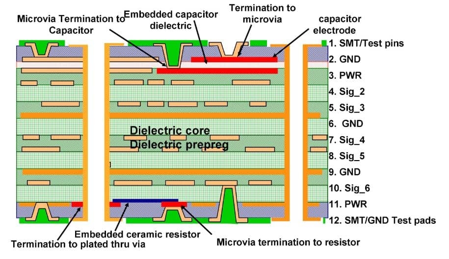
For those advancing beyond single-layer designs, copper pour and grounding become even more critical in multi-layer PCBs. In a typical four-layer board, the inner layers are often dedicated to power and ground planes. These continuous copper planes provide a low-impedance path for currents and shield signals on outer layers from interference.
As a beginner, remember that copper pour on outer layers should connect to inner ground planes through vias. This technique, called via stitching, ensures a consistent ground reference across the board. For example, in a design with a 1 GHz signal, improper grounding between layers can increase return path impedance by over 50 mΩ, leading to signal degradation. Proper via stitching can reduce this to under 5 mΩ.
Start with small multi-layer projects to practice these concepts. Focus on maintaining clean connections between layers and avoiding gaps in ground planes.
Best Practices for Copper Pour and PCB Grounding
To wrap up this intro to copper pour and grounding guide, here are some best practices for beginners to follow in every design:
- Prioritize Ground Planes: Whenever possible, dedicate an entire layer or large area to ground. This creates a stable reference and minimizes noise.
- Use Via Stitching for High-Speed Designs: For frequencies above 10 MHz, stitch ground pours across layers with vias to keep impedance low.
- Balance Copper Distribution: Ensure copper pour is roughly equal on all layers to prevent warping during manufacturing.
- Check for Isolation: Use design rule checks in your software to spot unconnected copper areas and fix them before production.
- Consider Thermal Reliefs: When connecting copper pour to component pads, use thermal relief patterns (small gaps with thin connections) to make soldering easier. Without reliefs, large copper areas can act as heat sinks, making soldering difficult.
Following these practices will help you create reliable, efficient designs as you grow in your PCB journey.
Conclusion: Mastering Copper Pour and Grounding for Better Designs
Understanding copper pour basics and having PCB grounding explained in simple terms is a game-changer for beginners. Copper pour isn’t just about filling empty space—it’s a strategic tool to reduce noise, improve power delivery, and manage heat. Grounding, meanwhile, provides the foundation for stable and safe operation of your circuits.
By following this copper fill tutorial and applying the tips for simple PCB design, you can avoid common mistakes and build better boards. Start small, experiment with copper pour in your projects, and always prioritize a solid grounding strategy. With practice, these concepts will become second nature, paving the way for more complex and successful designs.
At ALLPCB, we’re committed to supporting your journey in PCB design with resources and expertise. Keep exploring, and watch your skills grow with every project!
 ALLPCB


