ALLPCB


Overview
Memory chips are a category of integrated circuits within the semiconductor industry and are among the most widely used and standardized foundational IC products. Semiconductors can be classified by product type into optoelectronic devices, sensors, discrete devices and integrated circuits. Integrated circuits account for the largest share of semiconductor value, and include analog chips, microprocessor chips, logic chips and memory chips.
Types of storage devices
Storage devices are hardware components used to store and retrieve data. Based on storage medium they can be classified as optical storage, magnetic storage and semiconductor storage.
Optical storage uses optical methods to read and write data on optical media, such as optical disc drives, tape drives and optical card devices.
Magnetic storage uses magnetic media to store information; read and write processes rely on mechanical movement of magnetic platters and are widely used in PC hard drives and external hard disks.
Semiconductor storage, or memory chips, store information using electrical charge in semiconductor materials. Read and write operations are performed by storing or releasing electrons. Semiconductor storage is widely used in system memory, USB flash drives, consumer electronics, smart devices and solid-state drives.
Volatile vs non-volatile memory
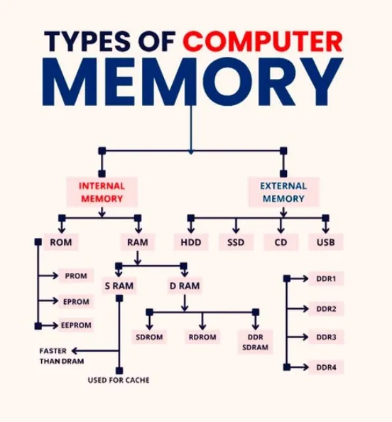
Memory chips are broadly classified by whether they retain data after power is removed: volatile memory (RAM) and non-volatile memory (ROM).
RAM is random-access memory that does not retain data when power is removed. Major RAM types include SRAM and DRAM. DRAM (dynamic random-access memory) stores each bit using a capacitor and a transistor. Because capacitors leak charge, DRAM cells require periodic refresh to preserve data. SRAM (static random-access memory) uses a more complex internal structure and can retain data without refresh as long as power is applied.
ROM stores fixed information that can be read but not modified or rewritten during normal operation. ROM retains data when external power is cut off. Types include EEPROM (electrically erasable programmable read-only memory), flash memory, PROM (programmable ROM) and EPROM (erasable programmable ROM).
Memory hierarchy in computer systems
Computer memory can be divided into six layers: registers, cache, main memory, disk cache, fixed disk and removable storage. From CPU cache and system RAM to SD cards and HDDs, the storage hierarchy is organized so that each layer exchanges data mainly with adjacent layers. From top to bottom, capacity increases, distance from the CPU increases, access speed decreases, transfer latency grows, and cost per byte declines.
Registers in the CPU (L0) are implemented using SRAM, integrated inside the CPU with very limited capacity and extremely high speed. Cache is a small, fast memory typically implemented in SRAM and often integrated in the CPU as a buffer for DRAM. Main memory is usually DRAM, offering higher density and larger capacity than SRAM but lower speed. In summary, SRAM is expensive and fast, DRAM is cheaper with larger capacity but slower, and external storage such as SSDs and HDDs provides much larger capacity at lower cost and with higher access latency.
DRAM and flash
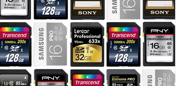
DRAM and flash are the dominant memory chip types in the market. Flash memory is divided into NOR and NAND types. The difference lies in how storage cells are connected, affecting read, erase and write behavior. NAND typically multiplexes pins and has slower random-read performance than NOR but much faster erase and write speeds. NAND circuitry is simpler, enabling higher data density, smaller form factor and lower cost, so large-capacity flash products (for example SSDs, USB flash drives, and SD cards) generally use NAND.
Compared with flash, DRAM provides higher read/write speed and shorter storage retention but at higher cost per bit. DRAM is mainly used for PC memory (e.g., DDR), mobile memory (e.g., LPDDR) and server memory.
Industry supply chain
Upstream participants include semiconductor material suppliers (silicon wafers, photoresist, target materials, polishing materials, specialty electronic gases) and semiconductor equipment suppliers (lithography, PVD, CVD, etch, cleaning, packaging and test equipment).
Midstream consists of memory chip manufacturers responsible for design, fabrication and packaging/test, producing DRAM, NAND flash and NOR flash chips.
Downstream are application industries such as consumer electronics, automotive electronics, communications and artificial intelligence. Various electronic and intelligent devices rely on memory chips.
Related Reading: Memory Chip Technology Trends
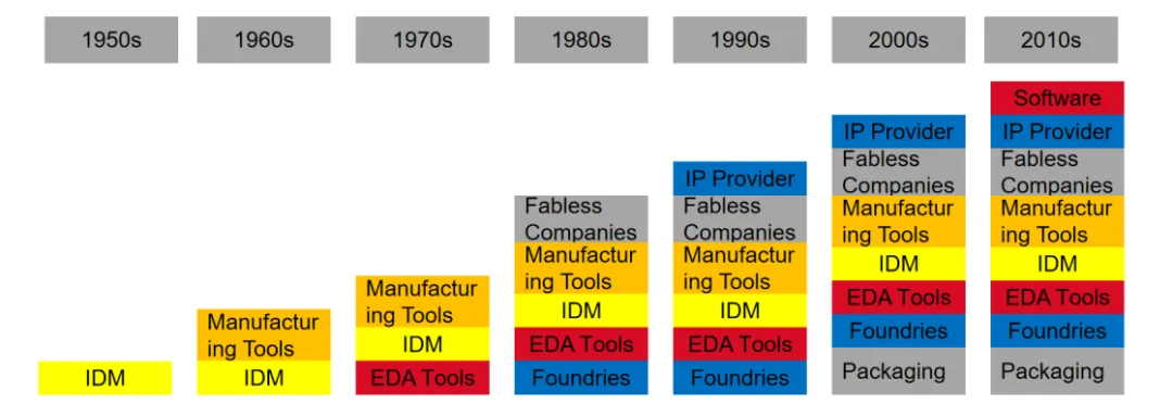
Business models: IDM and vertical specialization
The memory chip value chain includes IC design, wafer manufacturing, packaging and testing, and module integration. From an operating model perspective, the industry is mainly split between IDM and vertically specialized models.
IDM (Integrated Device Manufacturer) refers to companies that cover IC design, manufacturing, packaging and testing internally. Many large international memory companies operate as IDMs.
The vertical specialization model separates functions into fabless design companies, foundries (wafer fabs) and OSATs (outsourced packaging and testing). Fabless companies focus on IC design and sales and outsource manufacturing and packaging, while foundries specialize in chip fabrication.
Historically, the semiconductor industry began with IDM-only operations. Over decades the global industry has evolved toward specialization and integration across separate entities.
DRAM families: DDR, LPDDR, GDDR
DDR, LPDDR and GDDR are DRAM families defined to meet different application power, performance and form factor requirements. JEDEC defines DRAM standards to help designers meet target application specifications.
Standard DDR targets servers, cloud, networking, laptops, desktops and consumer applications, supporting wider channel widths, higher densities and multiple form factors. Performance improvements historically come from increasing core frequency.
Mobile DDR (LPDDR) targets mobile devices and automotive applications that are highly sensitive to power and form factor, offering narrower channel widths and various low-power modes. LPDDR evolved from DDR standards prior to DDR4 and has seen application-driven development since then, with performance improvements achieved through larger prefetch sizes.
Graphics DDR (GDDR) targets high-throughput, data-intensive applications such as graphics, data-center acceleration and AI. GDDR is used in high-end graphics cards and emphasizes wide data buses and much higher operating frequencies than contemporaneous DDR.
NAND flash cell types
By cell density, NAND flash is classified as SLC, MLC, TLC and QLC.
SLC (single-level cell) stores 1 bit per cell, offering the best performance and endurance—up to about 100,000 P/E cycles—but lower capacity and higher cost. SLC is used where high endurance is required, such as certain server and defense applications.
MLC (multi-level cell) stores 2 bits per cell, providing higher data density and larger capacity than SLC, with endurance around 10,000 P/E cycles.
TLC (triple-level cell) stores 3 bits per cell, with reduced performance and endurance (up to about 3,000 P/E cycles) but significantly higher capacity and lower cost, making it widely used in consumer products where a balance of performance, price and capacity is desired.
QLC (quad-level cell) stores 4 bits per cell, with further reduced performance and endurance (around 1,000 P/E cycles) but lower cost and higher capacity per cell. Many consumer high-capacity SSDs use QLC NAND.
Related Reading: ONFI: NAND Flash Interface Explained
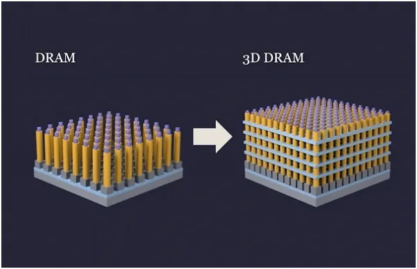
2D NAND vs 3D NAND and architectures
2D NAND places storage cells side by side on the substrate, which limits the available cell area and reduces reliability when cells are scaled down. 3D NAND stacks cells vertically, increasing transistor count per unit area and enabling higher storage density and capacity with improved endurance and power efficiency without drastic price increases.
Market 3D NAND architectures include traditional planar array designs and CMOS-under-array (CuA) architectures. In 2018, Yangtze Memory announced a 3D NAND architecture called Xtacking that uses wafer bonding as a key technology to separate CMOS logic from the stacked NAND array.