ALLPCB


Introduction
Creating a lithium-ion charger through a DIY electronics project offers hobbyists an engaging way to combine circuit design, PCB fabrication, and assembly skills. This weekend endeavor focuses on producing a basic charger board that safely manages charging cycles for common lithium-ion cells. The process emphasizes hands-on techniques such as PCB etching via the toner transfer method and careful component placement. Participants gain practical experience while learning fundamental principles of reliable board construction. Such projects build foundational knowledge applicable to more advanced electronic builds.
Why a Custom Lithium-Ion Charger PCB Matters for Hobbyists
A dedicated lithium-ion charger PCB allows precise control over charging parameters, reducing risks associated with improper voltage or current delivery. Hobbyists often work with rechargeable cells in portable devices, robots, or custom power systems, where off-the-shelf solutions may lack flexibility. Building the board in-house supports experimentation with layouts tailored to specific enclosure sizes or component arrangements. This approach also reinforces understanding of how board quality influences long-term performance and safety. Following established practices helps ensure the finished assembly meets basic reliability expectations.
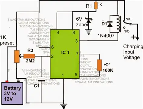
Technical Principles of Lithium-Ion Battery Charging Circuits
Lithium-ion cells require a constant-current followed by constant-voltage charging profile to reach full capacity without overcharging. The circuit typically incorporates a control element that monitors cell voltage and limits current once the target threshold is approached. Protection features such as over-voltage cutoff and thermal monitoring prevent damage during operation. Board layout must account for trace widths sufficient to carry expected currents while minimizing resistance and heat buildup. Proper grounding and separation of power and signal paths further contribute to stable performance. These mechanisms align with general engineering considerations for safe energy management in small-scale applications.
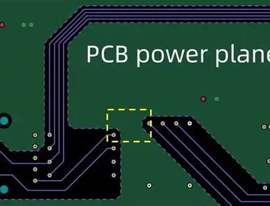
PCB Design Considerations for the Charger Project
Effective PCB design begins with a clear schematic that maps connections between the charging controller, input connector, output terminals, and any status indicators. Component placement prioritizes short power traces and adequate spacing for heat dissipation. Hobbyists commonly use single-sided or double-sided copper clad boards for simplicity in a weekend timeline. Design rules include maintaining minimum trace widths based on current requirements and ensuring sufficient clearance between conductors. Logical organization of the layout reduces the chance of assembly errors later. Visual inspection of the finished design helps identify potential issues before fabrication begins.
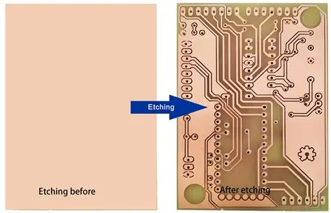
Fabricating the Board with the Toner Transfer Method
The toner transfer method provides an accessible route for hobbyists to create custom PCBs without specialized equipment. It starts with printing the circuit pattern onto transfer paper using a laser printer, followed by aligning and ironing the paper onto a clean copper clad board. After cooling, the paper is soaked away to leave the toner as an etch resist. The board then undergoes etching in a ferric chloride or similar solution to remove unprotected copper. Thorough rinsing and resist removal complete the process, yielding a functional board ready for drilling. Attention to even heating and clean surfaces improves transfer quality and reduces defects.
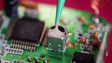
Soldering Tutorial and Component Assembly Best Practices
Soldering the components demands steady technique and appropriate tools to achieve reliable joints. Begin by securing the board and populating parts in order of height, starting with low-profile resistors and capacitors. Apply flux to pads, heat the joint evenly with a temperature-controlled iron, and feed solder until a smooth fillet forms. Avoid excessive heat dwell times that could damage sensitive components or lift pads. After placement, inspect each connection under good lighting for bridges, cold joints, or incomplete wetting. Cleaning residual flux completes the assembly stage and prepares the board for testing.
Testing, Troubleshooting, and Safety Insights
Initial testing involves verifying continuity with a multimeter before applying power, followed by gradual voltage ramp-up while monitoring current draw. Common issues such as open traces or reversed polarity can be isolated through systematic checks. Hobbyists benefit from documenting measurements at each stage to identify deviations early. Safety considerations include using appropriate enclosures, fuses on input lines, and never leaving charging cells unattended. These steps help confirm the charger operates within expected parameters and supports safe cell handling.
Conclusion
A weekend lithium-ion charger PCB project combines accessible fabrication techniques with core electronics principles to deliver a functional, custom solution. Through toner transfer etching, careful soldering, and methodical testing, hobbyists develop skills that extend to future DIY electronics projects. Attention to layout, process control, and verification contributes to boards that perform consistently. This hands-on experience reinforces the value of structured approaches in personal electronic builds.
FAQs
Q1: What safety features should a basic lithium-ion charger PCB include?
A1: A simple lithium-ion charger circuit typically incorporates voltage monitoring and current limiting to prevent overcharge conditions. Hobbyists often add thermal protection and reverse polarity safeguards during the design phase. These elements help maintain cell integrity throughout the charging cycle while aligning with general best practices for DIY electronics projects.
Q2: How does the toner transfer method support a weekend PCB etching project?
A2: The toner transfer method enables rapid creation of custom boards using common household tools and readily available materials. It involves printing the layout, transferring the pattern to copper clad stock, and etching away unwanted areas. This approach keeps the entire fabrication process manageable within a short timeframe for most electronic hobbyists.
Q3: What soldering techniques improve results in a DIY electronics project?
A3: Effective soldering starts with clean surfaces, proper flux application, and controlled iron temperature to form consistent joints. Working methodically through component installation and inspecting each connection reduces defects. These practices contribute to reliable assemblies in projects such as a lithium-ion charger PCB.
Q4: Why is PCB layout important when building a lithium-ion charger?
A4: Thoughtful PCB layout ensures adequate trace widths for current handling and proper component spacing for heat management. It also minimizes noise and supports stable operation of the charging circuit. Hobbyists who prioritize these factors often achieve better performance from their finished DIY electronics project.
References
IPC-6012E — Qualification and Performance Specification for Rigid Printed Boards. IPC, 2017
IPC-A-600K — Acceptability of Printed Boards. IPC, 2020
J-STD-001 — Requirements for Soldered Electrical and Electronic Assemblies. IPC