ALLPCB


Introduction
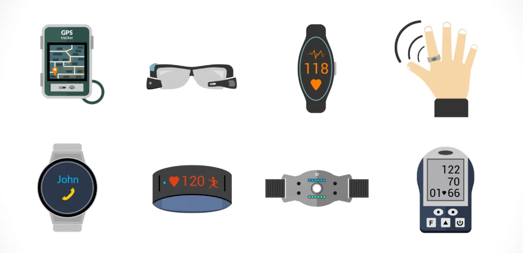
Driven by portable and wearable-device requirements, many designs are moving toward supply voltages of 3.6 V or lower. However, some functions in these devices require higher voltages, so designers use DC-DC boost converters implemented for optimum efficiency to step up to the required voltage.
This article reviews the purposes of DC-DC boost regulators and describes common topologies. It also discusses example devices and the design techniques and trade-offs needed to develop efficient designs for portable and wearable applications.
Role of DC-DC Boost Converters
Typical wearable and portable devices use lithium-ion batteries with a nominal output of about 3.6 V DC. Most battery-powered applications rely on one or more series lithium-ion cells to provide the primary supply voltage. While this is sufficient for most functions, certain features in laptops, tablets, and other mobile devices require higher voltages.
Examples include white LED backlight drivers, RF transceivers, precision analog circuits, and the bias circuits for avalanche photodiodes (APDs) in optical receivers. Boost DC-DC regulators convert low input voltages to higher output voltages to meet these requirements.
Typical Boost Converter Topologies
Key components of a boost regulator include an inductor, semiconductor switches (commonly power MOSFETs), a rectifier diode, an IC control block, and input and output capacitors.
When VIN is applied and the power switch is closed, current flows along the path that charges the inductor to ground. The inductor stores energy in its magnetic field. The diode is reverse-biased and the output capacitor discharges as its stored energy supplies the load.
Conversely, when the power switch opens, the collapsing magnetic field produces a positive voltage that, through the forward-biased diode, transfers inductor energy to charge the output capacitor and supply the load.
The control block maintains a constant output voltage by varying the switch duty cycle in response to input voltage and load changes. An output resistor divider provides voltage feedback to the control block to regulate the duty cycle and hold the desired output voltage.
Integrated designs often include optional protection features for overtemperature, output short-circuit, open-load conditions, and input overcurrent.
A common improvement on the basic circuit is replacing the diode with a second MOSFET. The second MOSFET functions as a synchronous rectifier, conducting when the power switch is off. Its lower voltage drop reduces power dissipation and improves regulator efficiency.
Higher efficiency translates to longer battery life in battery-powered devices, making synchronous designs advantageous. Portable and wearable devices are space-constrained, so boost converters targeted at these applications are highly integrated. Including power components inside the package limits current capability, but this trade-off is often acceptable in battery-powered designs. Many such applications spend long periods in shutdown, so ultra-low quiescent current is critical.
For example, the TPS610993YFFT from Texas Instruments is a low-power boost regulator that integrates a synchronous design with a quiescent current of only 1 μA while supplying up to 800 mA and producing 3.0 V output from inputs as low as 0.7 V. The device is designed to maximize efficiency at light loads and can be used with primary or rechargeable batteries such as NiMH or lithium-ion cells.
The TPS610993 integrates the power switch and synchronous rectifier in a 6-ball wafer-level chip-scale package (WCSP) measuring 1.23 mm x 0.88 mm. Its small size makes it suitable for space-constrained applications such as optical heart-rate monitors and LCD bias drivers. The TPS61099x family supports output voltages from 1.8 V to 5.5 V.
For higher output voltages used by camera flash circuits or battery-powered LED drivers, Microchip Technology's MCP1665 uses a different approach: it integrates a 36 V, 100 mΩ NMOS power switch but uses an external diode in a non-synchronous topology.
The MCP1665 can source up to 1 A from a 5 V supply and includes features such as controlled startup voltage, selectable operating modes, and a 500 kHz switching frequency. Its peak-current-mode architecture achieves high efficiency across a wide load range.
In some boost applications, maintaining a fixed output voltage is not the primary goal. For LED backlight drivers, required brightness is a function of LED string current, so the current through a shunt resistor forms the feedback voltage for the controller and determines the boost voltage. Diodes Incorporated's AP3019AKTR-G1 is an example of an optimized boost converter for backlight applications, capable of driving up to eight LEDs in series.
The AP3019A is optimized for space-limited applications and integrates the power switch and diode with a 1.2 MHz switching frequency that allows the use of miniature external components. It comes in an SOT-23-6 package and can deliver up to 550 mA.
The CTRL pin is a dedicated shutdown and dimming input: applying 1.8 V or higher enables the device; 0.5 V or lower disables it. A PWM signal can be applied to control LED brightness.
Design Techniques to Optimize Efficiency
Manufacturers may fix some parameters internally, but designers must typically make trade-offs to optimize conversion efficiency and carefully select external components according to applicable guidelines.
Switching frequency: Although switching frequency does not directly affect output voltage, it strongly influences power-supply design. Generally, higher switching frequencies allow the use of smaller inductors and capacitors. Inductor size is mainly determined by the allowable ripple current. For a given inductor, ripple current decreases as switching frequency increases. If several devices are available, designers can balance a higher switching frequency against a smaller inductor while maintaining the same ripple current.
Higher operating frequency also provides greater bandwidth for switching regulators, reducing transient response time. Smaller inductors reduce supply size and cost.
Inductor selection: The inductor is a critical component in a boost converter: it stores energy while the power switch is on and transfers stored energy through the output rectifier diode to the output when the switch is off.
Designers must balance low inductor current ripple with high efficiency. For a given package, lower-inductance parts typically have higher saturation current and lower series resistance, but lower inductance leads to higher peak currents, which can reduce efficiency and increase ripple and noise.
When selecting an inductor, its rated saturation current must exceed the peak inductor current, and its RMS current rating must exceed the regulator's maximum DC input current.
Most regulator datasheets include recommendations for various load currents and voltages. For example, the MCP1665 datasheet recommends a 4.7 μH ELL-8TP4R7NB inductor from Panasonic for outputs below 15 V and a 10 μH 7447714100 inductor from Wurth Electronics for higher output voltages.
Diode Selection
In non-synchronous designs, use a Schottky diode with low forward voltage to reduce losses. The diode's average forward current rating must meet or exceed the maximum output current. Its repetitive peak forward current rating must meet or exceed the inductor peak current, and its reverse breakdown voltage must exceed the internal power switch rating.
For example, the MCP1665 integrates a 36 V internal switch and can deliver up to 1 A. Microchip recommends the STPS2L40VU Schottky diode from STMicroelectronics, which has a 40 V reverse breakdown voltage and 2 A forward current rating.
Diode leakage at high temperature can also significantly affect converter efficiency. For higher current and ambient temperature applications, choose a diode with good thermal characteristics.
Input and Output Capacitors
In a boost topology, the inductor reduces transient demands on the supply circuit, decreasing required input filtering. X5R-grade ceramic capacitors typically satisfy +85 °C operating requirements, but X7R capacitors with low ESR may be required for +125 °C operation.
If the source impedance is high and cannot keep the input voltage above the undervoltage lockout threshold during large load steps, additional electrolytic or tantalum capacitors may be necessary.
On the load side, output capacitors reduce load ripple and help maintain stable output voltage during load transients. X7R ceramic capacitors are recommended for output applications, as other types may have higher ESR that reduces converter efficiency.
Capacitors should have DC voltage ratings appropriately above the maximum VOUT, since ceramic capacitors can lose capacitance near their rated voltage. Consult the datasheet for specific capacitor selection guidance.
Layout Considerations for Boost Regulators
Boost regulators switch at high speed, so performance is highly sensitive to PCB layout: parasitic inductance and capacitance can cause high output ripple, poor regulation, excessive EMI, and even failures due to high-voltage spikes.
Designers should pay close attention to PCB layout and apply the following practices:
- Place output capacitors close to the device and use short, wide traces to minimize parasitic inductance that can cause voltage ringing and spikes. Multiple vias can reduce parasitic inductance further.
- After placing the output capacitor, place the inductor near the IC to reduce generated EMI. The SW node is electrically noisy; route feedback (FB) and other sensitive traces away from this node.
- Route the input capacitor return close to the IC power ground pin to minimize loop area.
- For optimal thermal performance, include thermal vias from the device heatsink pad (if applicable) to the ground plane to improve heat dissipation and reduce the risk of thermal shutdown.
- Tie power ground, signal ground, and the thermal pad together at a single low-impedance point.
Online Design Tools Accelerate Development
Efficient power supply design requires expertise across component evaluation and selection, magnetics, compensation network design, optimization, thermal analysis, and layout. Recognizing this complexity, several power semiconductor suppliers provide online design tools to guide engineers through the necessary steps for a successful design.
For example, Texas Instruments provides tools such as Power Stage Designer to assist engineers in designing common switching power stages. For boost converters, designers can choose boost, buck-boost, and SEPIC topologies. After selecting a recommended topology, the tool helps compare power FET performance, select bulk capacitors, determine compensation networks, and perform other design tasks.
Analog Devices provides the ADIsimPower design tool suite to generate schematics and bill-of-materials (BOM) and to calculate circuit performance. ADIsimPower can optimize designs for cost, board area, efficiency, and part count while considering IC and external component operating limits.
Conclusion
Boost regulators enable higher-voltage circuit functions in battery-powered portable and wearable device designs and play an important role in meeting system requirements. Designers must select devices appropriate for the intended boost application and pay attention to several key trade-offs and best practices.