ALLPCB


Are you looking for a reliable way to ensure your populated printed circuit board assemblies are working as intended? PCB functional testing is the key to systematically checking populated printed circuit board assemblies for performance and reliability. In this comprehensive guide, we’ll dive deep into the world of PCB functional testing, exploring its importance, methods, and best practices to help you achieve flawless results in your electronic projects.
Whether you're an engineer, a hobbyist, or a manufacturer, understanding how to test your boards effectively can save time, reduce costs, and prevent failures. Let’s explore everything you need to know about PCB functional testing and how it plays a critical role in ensuring quality.
What Is PCB Functional Testing and Why Does It Matter?
PCB functional testing is the process of verifying that a populated printed circuit board (PCB) operates according to its design specifications. Unlike other testing methods that focus on individual components or connections, functional testing evaluates the board as a whole, ensuring all parts work together seamlessly under real-world conditions.
Why is this important? Studies suggest that manufacturing defects can account for up to 20% of PCB failures. Without proper testing, these issues can lead to costly recalls, damaged reputations, or even safety hazards in critical applications like medical devices or automotive systems. By systematically checking populated printed circuit board assemblies, you can catch issues early and ensure your product meets quality standards.
In the following sections, we’ll break down the steps, tools, and techniques involved in PCB functional testing to help you implement a robust testing process.
The Importance of Systematically Checking Populated Printed Circuit Board Assemblies
When a PCB is populated with components like resistors, capacitors, and integrated circuits, even a small error—such as a misplaced component or a soldering defect—can cause the entire board to fail. Systematically checking populated printed circuit board assemblies through functional testing ensures that every element works together as intended.
This process involves simulating the board’s real operating environment to verify performance. For example, if your PCB is designed for a power supply with an output of 12V and a current of 2A, functional testing will confirm whether it delivers those exact values under load. Without this step, you risk deploying a product that fails in the field, leading to costly rework or customer dissatisfaction.
Functional testing also helps identify issues that other methods, like visual inspection or automated optical inspection (AOI), might miss. These methods can detect physical defects but cannot confirm whether the board performs its intended function. That’s why a systematic approach to testing is critical for quality assurance.
Key Steps in PCB Functional Testing
To ensure your PCB performs as expected, follow these key steps for systematically checking populated printed circuit board assemblies. Each step builds on the last, creating a thorough testing process.
1. Define Test Requirements and Specifications
Before testing begins, you must clearly define what “success” looks like for your PCB. This means reviewing the design specifications and identifying key performance metrics. For instance, if your board is part of a communication device, you might test for signal integrity at specific frequencies, such as 2.4 GHz for Wi-Fi signals, or measure latency in microseconds.
Create a detailed test plan that outlines the inputs, expected outputs, and environmental conditions (like temperature or humidity) under which the board should operate. This plan serves as your roadmap for testing and ensures consistency across multiple boards.
2. Prepare the Testing Environment
Setting up the right environment is crucial for accurate results. This includes using the appropriate power supplies, signal generators, and measurement tools like oscilloscopes or multimeters. For example, if your PCB is designed to handle high-speed signals, ensure your testing equipment can measure rise times in nanoseconds to detect any signal degradation.
Additionally, simulate real-world conditions as closely as possible. If your board will operate in a high-temperature environment, such as an industrial setting at 85°C, perform testing under similar conditions to validate performance.
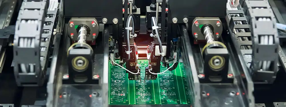
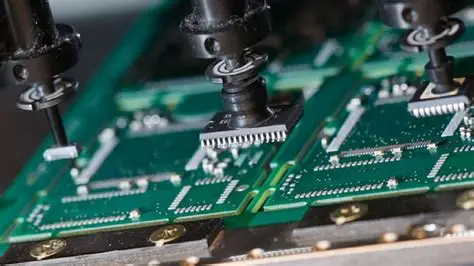
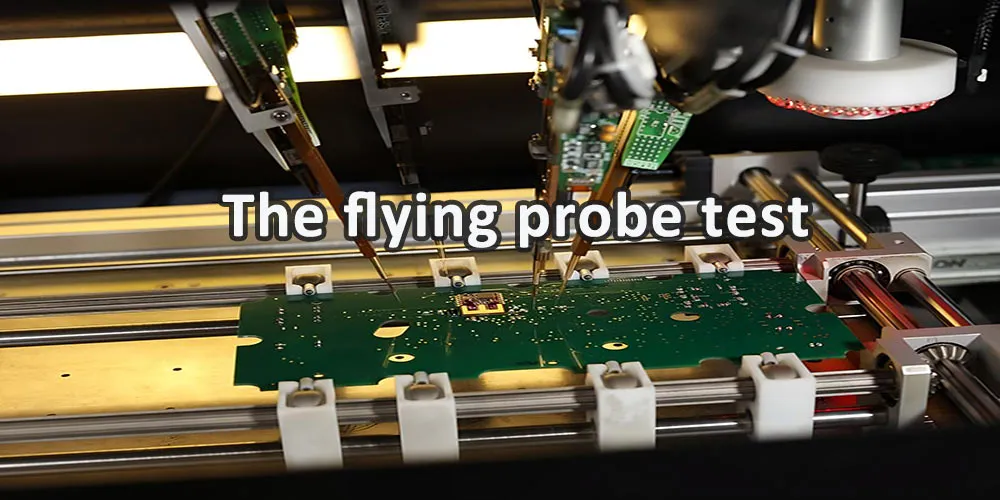
3. Develop or Use Test Fixtures
A test fixture is a custom device or setup that connects your PCB to testing equipment. It ensures consistent contact with test points on the board, making it easier to systematically check populated printed circuit board assemblies. Test fixtures are especially useful for high-volume production, as they speed up the process and reduce human error.
For example, a bed-of-nails fixture uses spring-loaded pins to make contact with specific points on the PCB, allowing you to test multiple signals or voltages simultaneously. Ensure that your fixture aligns with the board’s design and test points for accurate measurements.
4. Execute Functional Tests
With everything in place, it’s time to run the tests. Apply the defined inputs (such as voltage levels or signal patterns) and measure the outputs against your specifications. For instance, if your PCB controls a motor, test whether it delivers the correct RPM at a given input voltage, such as 5V producing 1000 RPM.
Use automated testing software when possible to log results and flag any deviations. This not only saves time but also provides a detailed record for troubleshooting or quality control.
5. Analyze Results and Troubleshoot Issues
After testing, review the data to identify any failures or anomalies. If a board doesn’t meet specifications—for example, if a voltage regulator outputs 4.8V instead of the expected 5V—trace the issue back to its source. This could involve checking for soldering defects, incorrect component values, or design flaws.
Use tools like thermal imaging cameras to detect overheating components or multimeters to measure impedance across traces (typically in milliohms) for potential shorts or opens. Address any issues before moving to the next batch of boards.
Common Methods for PCB Functional Testing
There are several approaches to systematically checking populated printed circuit board assemblies. Choosing the right method depends on your board’s complexity, production volume, and budget. Below are some of the most widely used techniques.
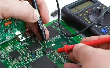
Manual Functional Testing
In manual testing, a technician uses tools like multimeters or oscilloscopes to check the board’s performance. This method is ideal for prototypes or low-volume production, as it allows for detailed inspection but can be time-consuming. For example, manually measuring a signal’s amplitude at 1V peak-to-peak ensures it meets design requirements.
Automated Functional Testing
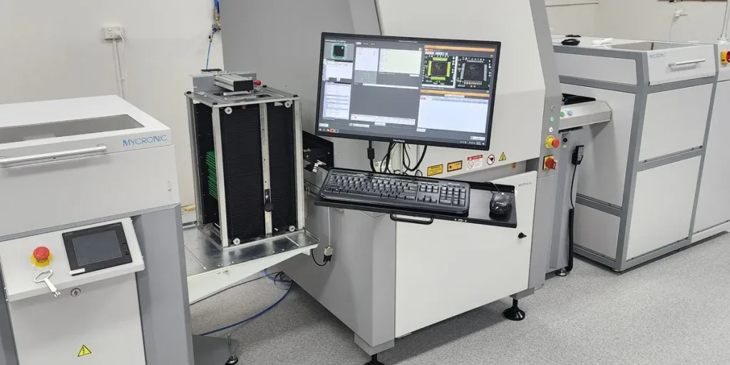
Automated testing uses specialized equipment and software to perform checks quickly and consistently. It’s ideal for high-volume production, where testing hundreds of boards manually would be impractical. Automated systems can simulate inputs, measure outputs, and log results with minimal human intervention, ensuring precision down to microvolt levels for sensitive circuits.
Boundary Scan Testing
Boundary scan testing, based on the JTAG (Joint Test Action Group) standard, is used for digital circuits. It checks for connectivity and functionality by accessing internal nodes of integrated circuits without physical probes. This method is particularly useful for complex boards with limited test point access, ensuring thorough verification of signal paths.
Best Practices for Effective PCB Functional Testing
To maximize the effectiveness of your testing process, follow these best practices for systematically checking populated printed circuit board assemblies.
- Design for Testability (DFT): During the design phase, include test points and access ports to make functional testing easier. For instance, place test pads for critical signals to measure voltages or frequencies directly.
- Standardize Testing Procedures: Create consistent protocols for testing to ensure repeatability, especially in production environments. Document every step, from setup to data analysis.
- Use Realistic Test Conditions: Test under conditions that mimic the board’s final application. If it’s for an outdoor device, test across a temperature range like -20°C to 60°C to validate performance.
- Invest in Quality Equipment: High-precision tools, such as oscilloscopes with bandwidths of 100 MHz or higher, ensure accurate measurements for high-speed signals.
- Iterate and Improve: Use test results to refine your design or manufacturing process. If a recurring issue like signal crosstalk at 50 MHz is detected, adjust trace spacing or shielding in future revisions.
Challenges in PCB Functional Testing and How to Overcome Them
While functional testing is essential, it comes with challenges. Here’s how to address common obstacles when systematically checking populated printed circuit board assemblies.
Complex Designs: Modern PCBs often have high component density and limited access to test points. Use advanced methods like boundary scan or automated fixtures to test without physical probes.
Time Constraints: Testing can be time-intensive, especially for large batches. Invest in automated testing systems to speed up the process without sacrificing accuracy.
Cost Considerations: High-quality testing equipment can be expensive. Start with essential tools for your specific needs, such as a multimeter for basic voltage checks, and scale up as your budget allows.
Environmental Variability: Test results can vary based on temperature or humidity. Use environmental chambers to control conditions and ensure consistent outcomes, especially for boards operating in harsh environments.
Conclusion: Ensuring Quality through PCB Functional Testing
PCB functional testing is a vital step in systematically checking populated printed circuit board assemblies to ensure they meet design specifications and perform reliably in real-world applications. By following a structured approach—defining test requirements, preparing the right environment, using appropriate methods, and adhering to best practices—you can catch defects early, reduce costs, and deliver high-quality products.
At ALLPCB, we understand the importance of quality in every stage of PCB production. Whether you’re working on a prototype or mass production, implementing a robust functional testing process is key to success. Use the insights and steps outlined in this guide to enhance your testing strategy and achieve consistent, reliable results for your electronic projects.