ALLPCB


In the world of electronics manufacturing, creating high-quality printed circuit boards (PCBs) is a critical process that involves several intricate steps. One of the most vital stages is PCB lamination, especially when dealing with multilayer boards that incorporate several layers, copper foil, and a substrate. If you're a manufacturer looking to understand the device used to create PCBs and the detailed lamination process, you've come to the right place. This guide will walk you through the essentials of PCB lamination, the equipment involved, and best practices to ensure optimal results.
In this comprehensive blog, we'll dive deep into the PCB lamination process, explore the tools and devices used, and provide actionable insights for manufacturers who aim to produce reliable and efficient multilayer boards. Whether you're new to PCB production or looking to refine your techniques, this guide will equip you with the knowledge you need.
What Is PCB Lamination and Why Is It Important?
PCB lamination is the process of bonding multiple layers of materials together to form a single, cohesive printed circuit board. These layers typically include copper foil for conductive pathways and a substrate (often made of materials like FR-4, a fiberglass-reinforced epoxy) for structural support and insulation. The lamination process ensures that these layers are securely fused, creating a stable foundation for electronic components.
For manufacturers, lamination is crucial because it directly impacts the durability, functionality, and performance of the final PCB. A well-laminated board can withstand thermal and mechanical stress, prevent delamination (separation of layers), and maintain signal integrity across complex circuits. Poor lamination, on the other hand, can lead to issues like warping, short circuits, or complete board failure.
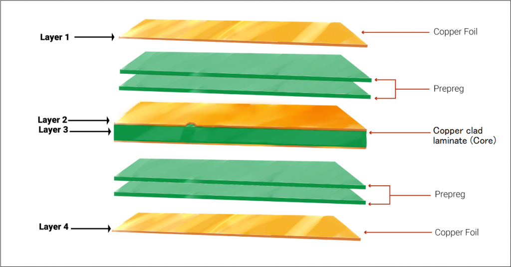
Understanding the Components of a Multilayer PCB
Before diving into the lamination process, it's helpful to understand the basic components that make up a multilayer PCB:
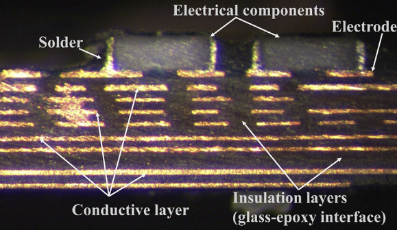
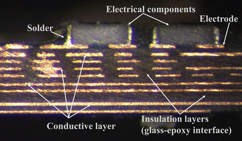
- Copper Foil: Thin sheets of copper that form the conductive pathways for electrical signals. These are typically 0.5 to 2 ounces per square foot in weight, translating to thicknesses of about 17 to 70 micrometers.
- Substrate: The insulating material that provides structural support. FR-4 is the most common substrate due to its balance of cost, durability, and thermal resistance (with a glass transition temperature, Tg, around 130-140°C).
- Prepreg: A partially cured resin material used to bond layers together during lamination. It acts as an adhesive and insulator between copper layers.
Multilayer PCBs can have anywhere from 4 to over 20 layers, depending on the complexity of the design. Each additional layer increases the board's ability to handle intricate circuits, but it also adds challenges to the lamination process.
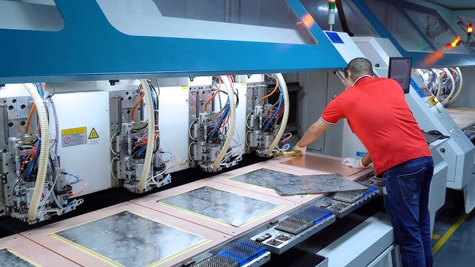
The Device Used to Create PCBs: Multilayer Press Machines
One of the primary devices used in the PCB lamination process is the multilayer press machine. This specialized equipment applies heat and pressure to bond the layers of copper foil, prepreg, and substrate into a single, unified board. Here's how it works:
- Stacking: Layers of copper foil, prepreg, and substrate are carefully aligned and stacked in the correct order based on the PCB design.
- Pressure Application: The multilayer press exerts uniform pressure, often between 200 to 500 psi (pounds per square inch), to ensure tight bonding between layers.
- Heat Application: The press also heats the stack to temperatures typically ranging from 170°C to 200°C. This activates the resin in the prepreg, allowing it to flow and cure, forming a solid bond.
- Cooling: After a set period (usually 1-2 hours), the press cools the stack under controlled conditions to prevent warping or stress in the board.
Modern multilayer presses often come with vacuum capabilities to remove air bubbles during lamination, which can otherwise cause defects. These machines are essential for manufacturers producing high-density interconnect (HDI) boards or designs with tight impedance control (e.g., maintaining 50 ohms for high-speed signals).
Step-by-Step Guide to the PCB Lamination Process
Now that we’ve covered the key device involved, let’s break down the PCB lamination process into clear, actionable steps for manufacturers working with several layers, copper foil, and a substrate.
1. Design and Preparation
The process begins long before the layers are stacked in a press. Manufacturers must start with a detailed PCB design that specifies the number of layers, material types, and stack-up configuration. This design dictates how the copper foil and substrate will be arranged and ensures that signal integrity (e.g., controlling impedance for differential pairs at 100 ohms) is maintained.
Once the design is finalized, materials are cut to size, and copper foil is etched to create the necessary circuit patterns for inner layers. This step often involves photolithography, where a photoresist layer is exposed to UV light through a mask to define the circuitry.
2. Layer Stacking and Alignment
With the inner layers prepared, the stack-up is assembled. This involves alternating layers of prepreg and copper-clad substrate, ensuring precise alignment to avoid misalignment of vias or traces. Registration pins or optical alignment systems are often used to achieve accuracy within 0.1 mm or better.
3. Lamination in the Multilayer Press
The aligned stack is placed into the multilayer press. As mentioned earlier, the press applies heat and pressure to bond the layers. The temperature and pressure profiles are carefully controlled based on the materials used. For instance, high-Tg materials (Tg above 170°C) may require higher temperatures to ensure proper resin curing.
During this stage, vacuum lamination may be employed to eliminate trapped air, which can cause voids or delamination. The process typically takes 1-2 hours, depending on the number of layers and material thickness.
4. Cooling and Post-Lamination Inspection
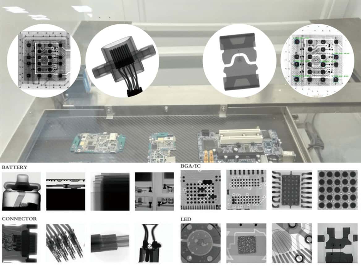
After lamination, the board is cooled under controlled conditions to prevent thermal shock, which could lead to warping. Once cooled, the board undergoes inspection for defects such as delamination, voids, or misalignment. Techniques like X-ray imaging or automated optical inspection (AOI) are often used to verify the integrity of the layers.
Sequential Lamination for Complex Designs
For advanced PCB designs, such as those used in high-density interconnect (HDI) applications, sequential lamination is often employed. This technique involves laminating subsets of layers in multiple steps rather than all at once. For example, a 12-layer board might be laminated in two stages: first, layers 1-6 are bonded, and then layers 7-12 are added in a second lamination cycle.
Sequential lamination allows for the creation of microvias (tiny holes with diameters as small as 0.1 mm) and buried vias, which are essential for compact, high-performance designs. However, it increases manufacturing time and cost due to the additional cycles in the multilayer press.
Common Challenges in PCB Lamination and How to Avoid Them
Even with advanced equipment, manufacturers may encounter challenges during the lamination process. Here are some common issues and tips to address them:
- Delamination: This occurs when layers separate due to poor bonding. To prevent it, ensure proper surface cleanliness before stacking (removing contaminants like dust or oil) and use the correct temperature and pressure settings for your materials.
- Warping: Uneven heating or cooling can cause the board to bend. Use a controlled cooling process and symmetrical stack-ups to balance stress across the board.
- Voids or Air Bubbles: Trapped air can weaken the bond between layers. Vacuum lamination is highly effective in minimizing this risk.
- Signal Integrity Issues: Misalignment or improper material selection can affect impedance (e.g., deviating from a target of 50 ohms for RF signals). Tight control over layer alignment and material dielectric constants (typically 4.2-4.5 for FR-4) is essential.
Choosing the Right Materials for PCB Lamination
The success of the lamination process heavily depends on the materials used. Here are key considerations for selecting copper foil, substrate, and prepreg:
- Copper Foil Thickness: Choose based on current-carrying requirements. For high-power applications, thicker foil (e.g., 2 oz or 70 micrometers) is ideal, while thinner foil (0.5 oz) suits high-density designs.
- Substrate Type: FR-4 is standard for most applications due to its cost-effectiveness and thermal stability. For high-frequency designs (e.g., above 1 GHz), consider low-loss materials with dielectric constants below 3.5.
- Prepreg Resin Content: Higher resin content ensures better flow and bonding during lamination, especially for thicker boards.
Impact of Lamination on Manufacturing Time and Cost
The lamination process can significantly affect the overall timeline and budget of PCB production. A single lamination cycle for a 4-layer board might take 1-2 hours, while sequential lamination for an HDI design could extend the process to several days. Additionally, the cost of materials (e.g., high-Tg substrates or specialized prepregs) and the need for vacuum presses can increase expenses.
Manufacturers can optimize costs by streamlining designs to minimize layer count where possible and investing in quality control to reduce rework due to lamination defects.
Best Practices for Manufacturers
To achieve consistent results in PCB lamination, consider these best practices:
- Invest in high-quality multilayer press equipment with vacuum capabilities for defect-free bonding.
- Maintain strict control over temperature (e.g., 180°C for standard FR-4) and pressure settings based on material specifications.
- Use automated alignment systems to ensure precision in layer stacking, especially for boards with 8 or more layers.
- Regularly calibrate equipment and inspect materials for consistency to avoid unexpected failures.
Conclusion: Mastering PCB Lamination for Quality and Efficiency
PCB lamination is a cornerstone of modern electronics manufacturing, enabling the creation of complex multilayer boards with several layers, copper foil, and a substrate. By understanding the role of the multilayer press—the primary device used to create PCBs—and following a structured lamination process, manufacturers can produce reliable, high-performance boards that meet the demands of today’s technology.
From material selection to overcoming common challenges like delamination and warping, this guide has covered the essential aspects of PCB lamination. By implementing the best practices outlined here, you can enhance the quality of your boards, reduce manufacturing defects, and ultimately deliver better products to your clients. Whether you're working on a simple 4-layer design or a complex HDI board, mastering the lamination process is key to success in PCB production.