 ALLPCB


If you're an engineer dealing with PCB lamination defects like delamination, voids, warpage, or registration issues, you're not alone. These problems can disrupt production, compromise quality, and increase costs. In this guide, we’ll break down the most common PCB lamination defects, their causes, and practical prevention tips to help you troubleshoot and improve your manufacturing process. Whether you're designing complex multilayer boards or overseeing production, this blog offers actionable insights to ensure your PCBs meet the highest standards.
Understanding PCB Lamination and Its Importance
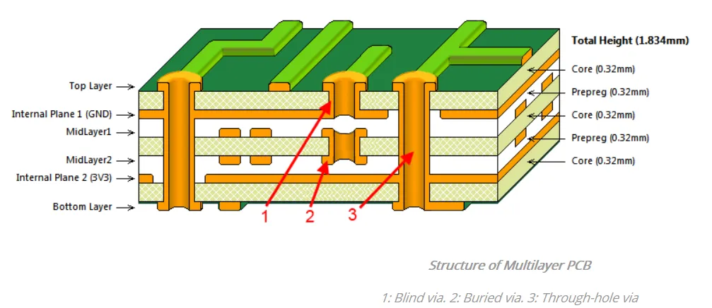
PCB lamination is a critical step in the manufacturing process where multiple layers of materials, including copper foil, prepreg (pre-impregnated resin), and core materials, are bonded together under heat and pressure. This process forms the foundation of multilayer printed circuit boards (PCBs), ensuring structural integrity and electrical performance. However, when lamination goes wrong, defects can arise, leading to failures in functionality or reliability.
Common PCB lamination defects include delamination, voids, warpage, and registration issues. These problems can result in signal integrity issues, mechanical failures, or even complete board rejection during testing. Understanding the root causes and implementing prevention strategies is essential for engineers aiming to produce high-quality PCBs.
Common PCB Lamination Defects: What to Look For
Before diving into troubleshooting, let’s identify the most frequent PCB lamination defects engineers encounter. Recognizing these issues early can save time and resources during production.
1. Delamination
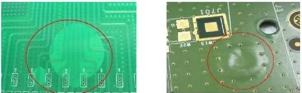
Delamination occurs when layers of the PCB separate due to poor bonding. This defect can appear as visible gaps or blisters between layers and often leads to electrical failures or mechanical weakness. Delamination is especially problematic in high-temperature environments where thermal stress exacerbates the separation.
2. Voids
Voids are air pockets or unfilled spaces within the laminated layers, often caused by trapped air or insufficient resin flow during the lamination process. These defects can weaken the board’s structure and interfere with signal transmission, especially in high-frequency applications where impedance control is critical (e.g., maintaining a 50-ohm impedance for RF signals).
3. Warpage
Warpage refers to the bending or twisting of a PCB after lamination, making it difficult to assemble components or fit the board into enclosures. Warped boards can also cause misalignment during soldering, leading to poor connections and reliability issues. Warpage often results from uneven thermal expansion or improper material selection.
4. Registration Issues
Registration issues happen when layers are misaligned during lamination, causing incorrect positioning of vias, traces, or pads. This defect can lead to open circuits, shorts, or failure to meet design specifications. For instance, a misalignment of just 0.1 mm in a high-density interconnect (HDI) board can render it unusable.
PCB Lamination Defect Causes: Why Do These Problems Happen?
Understanding the root causes of PCB lamination defects is the first step to effective troubleshooting. Here are the primary reasons these issues occur during the manufacturing process.
Causes of Delamination
- Moisture Contamination: Absorbed moisture in materials like prepreg or core can turn into steam during the high-temperature lamination process, weakening the bond between layers. Studies suggest that moisture levels above 0.2% by weight can significantly increase delamination risks.
- Poor Adhesion: Insufficient surface preparation, such as inadequate cleaning or roughening of copper foil, can prevent proper bonding with resin.
- Thermal Stress: Rapid heating or cooling during lamination can cause uneven expansion, leading to layer separation, especially in boards with mismatched coefficients of thermal expansion (CTE).
Causes of Voids
- Trapped Air: Inadequate vacuum pressure during lamination can leave air pockets between layers, forming voids.
- Insufficient Resin Flow: If the prepreg doesn’t have enough resin or if the lamination temperature is too low (e.g., below 180°C for standard FR-4 materials), the resin may not fill all gaps.
- Material Defects: Inconsistent prepreg quality or contamination can prevent uniform bonding.
Causes of Warpage
- Uneven Material Distribution: Asymmetrical stack-ups or unbalanced copper distribution across layers can cause differential shrinkage during cooling.
- Improper Cooling: Rapid or uneven cooling after lamination can induce stress, leading to bending. Ideally, cooling rates should be controlled at 2-3°C per minute for standard materials.
- Material Mismatch: Using materials with different CTE values (e.g., combining FR-4 with a high-Tg material) can result in warpage under thermal stress.
Causes of Registration Issues
- Equipment Misalignment: Inaccurate alignment tools or worn-out machinery can cause layers to shift during lamination.
- Material Shrinkage: Prepreg and core materials may shrink at different rates during heating (often by 0.5-1% for FR-4), leading to misalignment if not accounted for in design.
- Human Error: Incorrect handling or setup of lamination stacks can introduce errors in layer positioning.
PCB Lamination Defect Prevention: Practical Tips for Engineers
Preventing PCB lamination defects requires a combination of good design practices, material selection, and process control. Below are actionable strategies to minimize the risk of delamination, voids, warpage, and registration issues.
Preventing Delamination
- Control Moisture Levels: Store prepreg and core materials in a controlled environment (relative humidity below 50%) and bake them at 120°C for 2-4 hours before lamination to remove absorbed moisture.
- Enhance Surface Preparation: Ensure copper surfaces are clean and properly roughened (surface roughness of 1-2 μm is ideal for adhesion) to promote bonding with resin.
- Optimize Lamination Parameters: Use gradual heating and cooling profiles during lamination (e.g., ramp-up rates of 2-3°C per minute) to minimize thermal stress.
Preventing Voids
- Use Adequate Vacuum Pressure: Ensure the lamination press maintains a vacuum level of at least 25 inHg to remove trapped air during the process.
- Select High-Quality Materials: Choose prepreg with consistent resin content (typically 40-50% for FR-4) to ensure proper flow and gap filling.
- Monitor Lamination Temperature: Maintain temperatures within the recommended range for your material (e.g., 180-200°C for standard FR-4) to ensure resin flow without degradation.
Preventing Warpage
- Design Symmetrical Stack-Ups: Balance copper distribution across layers to avoid uneven stress. For example, mirror copper patterns on top and bottom layers of a 4-layer board.
- Control Cooling Rates: Implement slow, uniform cooling after lamination (2-3°C per minute) to reduce internal stress.
- Match Material Properties: Use materials with similar CTE values (e.g., FR-4 with a CTE of 14-17 ppm/°C) to minimize differential expansion.
Preventing Registration Issues
- Use Precision Equipment: Regularly calibrate lamination presses and alignment tools to ensure accuracy within 0.05 mm for high-density designs.
- Account for Shrinkage: Adjust layer artwork to compensate for material shrinkage (typically 0.5-1% for standard materials) during the design phase.
- Implement Quality Checks: Use X-ray inspection or automated optical inspection (AOI) post-lamination to detect misalignment early.
Troubleshooting PCB Lamination Defects: Step-by-Step Guide
When defects occur, a systematic approach to troubleshooting can help identify the root cause and implement corrective actions. Follow these steps to address PCB lamination issues effectively.
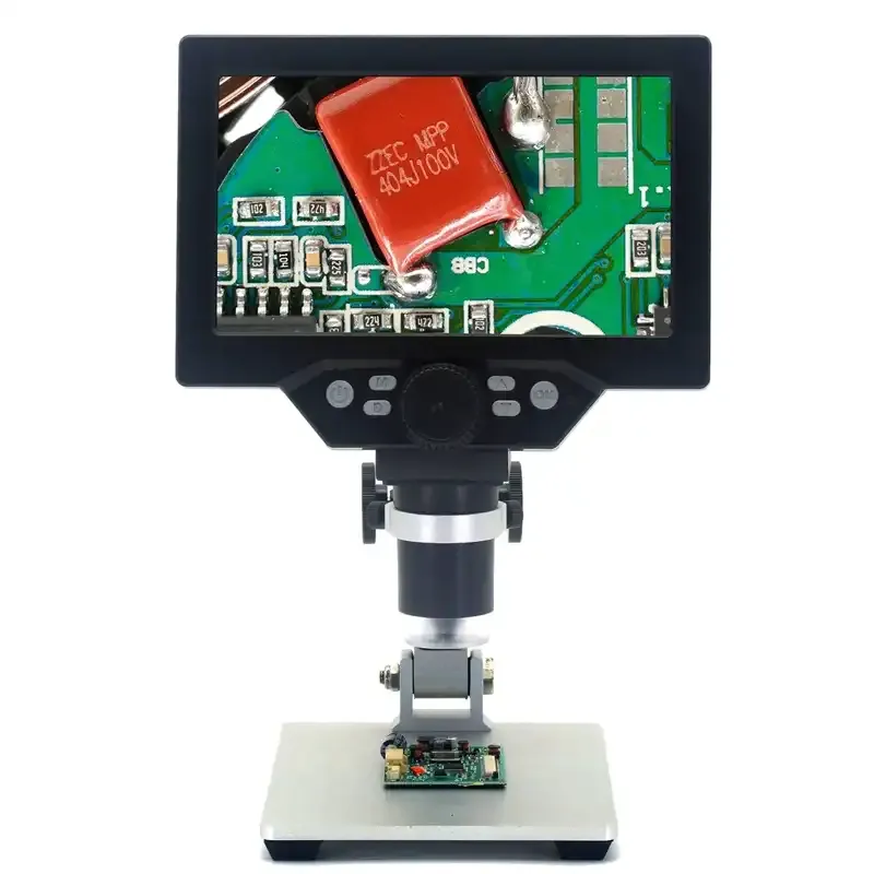
Step 1: Visual and Physical Inspection
Start by examining the PCB for visible signs of defects. Use a magnifying glass or microscope to check for delamination blisters, voids, or misalignment. Measure warpage using a flatness gauge to quantify the deviation (e.g., warpage exceeding 0.75% of board length is often unacceptable per IPC standards).
Step 2: Analyze Process Data
Review lamination process parameters such as temperature, pressure, and vacuum levels. Compare them against recommended values for your materials. For instance, if the temperature was below 180°C for FR-4, insufficient resin flow might be the cause of voids.
Step 3: Conduct Material Testing
Test prepreg and core materials for moisture content (using a moisture analyzer) and resin quality. High moisture levels (above 0.2%) or inconsistent resin content can point to material-related causes of delamination or voids.
Step 4: Use Advanced Inspection Techniques
Employ non-destructive testing methods like X-ray imaging to detect internal voids or misalignment. For delamination, acoustic microscopy can reveal hidden layer separation without damaging the board.
Step 5: Implement Corrective Actions
Based on your findings, adjust process parameters, improve material storage, or refine design rules. For example, if warpage is due to uneven copper distribution, redesign the stack-up for better symmetry.
Conclusion: Building Better PCBs Through Prevention and Troubleshooting
PCB lamination defects like delamination, voids, warpage, and registration issues can pose significant challenges for engineers, but they are manageable with the right knowledge and strategies. By understanding the causes of these defects—such as moisture contamination, improper process parameters, or material mismatches—you can take proactive steps to prevent them. Implementing best practices in design, material selection, and process control, along with systematic troubleshooting, ensures your PCBs achieve optimal performance and reliability.
At ALLPCB, we’re committed to supporting engineers with resources and expertise to overcome manufacturing challenges. By addressing PCB lamination defect causes and applying the prevention tips outlined in this guide, you can minimize production issues and deliver high-quality boards for any application. Keep refining your processes, and you’ll see consistent improvements in your PCB outcomes.


