 ALLPCB


In the fast-evolving world of electronics, high-density printed circuit boards (PCBs) are at the heart of modern devices, enabling compact designs with enhanced functionality. However, as PCB designs grow more complex with tighter tolerances and finer pitches, solder mask alignment becomes a critical challenge. Misalignment can lead to exposed copper, solder bridges, or compromised electrical performance, all of which jeopardize reliability. In this blog, we explore the intricacies of solder mask alignment in high-density PCBs, the challenges engineers face, and practical solutions to ensure precision and performance.
Understanding Solder Mask and Its Role in High-Density PCBs
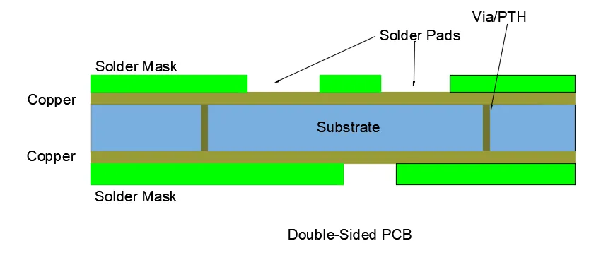
A solder mask, or solder resist, is a thin polymer layer applied to a PCB to protect copper traces from oxidation, prevent solder bridges, and ensure reliable soldering during assembly. In high-density PCBs, which feature fine-pitch components like ball grid arrays (BGAs) and chip-scale packages (CSPs) with pitches as low as 0.5 mm, the solder mask must be applied with extreme precision. The mask defines solderable areas, insulates conductive traces, and shields the board from environmental factors like moisture and dust.
In high-density designs, the solder mask's role extends beyond protection. It influences impedance control, crucial for high-frequency signals (e.g., 5G applications operating at 3-6 GHz), and ensures proper component placement. Misalignment, even by a few micrometers, can expose copper traces, leading to short circuits or signal integrity issues, or cover solder pads, hindering proper soldering.
Key Challenges in Solder Mask Alignment
1. Tight Tolerances in Fine-Pitch Designs
High-density PCBs often feature trace widths and spacing as small as 50-100 μm (2-4 mils). For comparison, standard PCBs may have trace widths of 150 μm or more. Solder mask openings must align precisely with these fine features, typically requiring clearances of 15-25 μm for high-density interconnect (HDI) boards. Misregistration by even 10 μm can expose adjacent traces, increasing the risk of solder bridging or short circuits during reflow soldering.
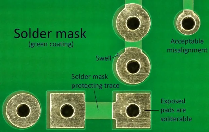
2. Solder Mask Misregistration
Solder mask misregistration occurs when the mask layer is not perfectly aligned with the copper pattern. This issue is particularly problematic in fine-pitch BGA/CSP applications, where pad sizes may be as small as 0.3 mm. According to industry standards like IPC-A-600, acceptable solder mask registration tolerances are typically ±50 μm for standard boards, but high-density designs demand tolerances as tight as ±25 μm. Misregistration can result in:
- Exposed copper: Leading to oxidation or unintended electrical connections.
- Covered pads: Preventing proper soldering and causing weak joints.
- Impedance variations: Affecting high-frequency signal performance (e.g., impedance shifts from 50 Ω to 55 Ω can degrade signal integrity in RF circuits).
3. Material and Process Limitations
The choice of solder mask material and application method significantly affects alignment accuracy. Liquid photoimageable solder masks (LPSM) are commonly used for their precision, but they can slump or spread during application, reducing edge definition. Dry film solder masks (DFSM), while offering uniform thickness, struggle with adhesion on uneven surfaces, common in HDI boards with stacked vias or thick copper (e.g., >3 oz for power electronics). Additionally, high copper thickness can cause stress on the solder mask, leading to cracking or peeling during thermal cycling, as noted in studies on heavy copper PCBs.
4. Thermal and Mechanical Stress
High-density PCBs often undergo multiple thermal cycles during reflow soldering, reaching temperatures up to 260°C. These cycles can cause differential expansion between the solder mask, copper, and substrate, leading to alignment shifts. For example, FR-4 substrates have a coefficient of thermal expansion (CTE) of ~14-17 ppm/°C, while solder masks typically range from 50-100 ppm/°C. This mismatch can cause the mask to shift or crack, especially in boards with high layer counts (e.g., 12-20 layers).
5. Complex Geometries and Via Tenting
HDI boards often incorporate microvias and blind vias, which require precise solder mask tenting to prevent solder or flux entrapment. Incomplete via tenting, where the solder mask fails to fully cover the via, can lead to chemical contamination or corrosion. Conversely, excessive solder mask in via openings can trap flux residues, reducing solder joint reliability. Achieving consistent tenting across thousands of vias on a single board is a significant challenge, particularly when via diameters are as small as 50 μm.
Image Suggestion: Include a close-up image of a PCB with microvias, showing proper and improper solder mask tenting to highlight the precision required.
Strategies to Overcome Solder Mask Alignment Challenges
1. Advanced Application Techniques
To address alignment issues, modern PCB manufacturing employs advanced techniques like Laser Direct Imaging (LDI). Unlike traditional photolithography, which uses film tools and UV exposure, LDI uses a laser to directly pattern the solder mask, achieving line resolutions below 30 μm. This precision is critical for HDI boards with fine-pitch components. Industry trials have shown LDI can reduce misregistration by up to 50% compared to conventional methods. Additionally, LDI eliminates the need for physical photomasks, reducing alignment errors caused by film misalignment.
2. Optimized Solder Mask Materials
Choosing the right solder mask material is crucial. LPSM, such as Taiyo's high-reliability inks, offers excellent adhesion and heat resistance, making it suitable for HDI boards. For heavy copper PCBs, selecting a solder mask with a lower CTE (e.g., 30-50 ppm/°C) can minimize thermal stress. Recent advancements in photosensitive solder masks have also improved edge definition, enabling finer patterns for pitches as low as 0.4 mm.
3. Design for Manufacturability (DFM) Guidelines
Implementing DFM guidelines can significantly improve solder mask alignment. Key recommendations include:
- Solder mask clearance: Maintain a clearance of 1.6-2 mils between pads and mask edges to account for potential misregistration.
- Solder dam width: Ensure a minimum solder dam width of 4 mils to prevent solder bridging.
- Expansion buffers: Oversize solder mask apertures by 75 μm per side to compensate for misalignment, as suggested by IPC-7351 standards.
- Fiducial markers: Incorporate registration markers on the copper layer to guide precise alignment during solder mask application.
Running a design rule check (DRC) before fabrication ensures that solder mask openings, clearances, and dams meet manufacturing capabilities. For example, a DRC can flag apertures smaller than 50 μm, which may be difficult to achieve with standard LPSM processes.
4. Enhanced Inspection and Quality Control
Post-application inspection is critical for high-density PCBs. Using automated optical inspection (AOI) systems with 10X-20X magnification ensures that solder mask alignment meets tolerances for fine-pitch components (e.g., 0.5-0.8 mm pitch). Additionally, capability studies (Cpk) on solder mask registration can quantify process reliability, with a Cpk ≥ 1.33 indicating a robust process. Regular sampling of chevron registration marks can further validate alignment accuracy.
5. Collaboration with Manufacturers
Close collaboration with PCB manufacturers during the design phase can preempt alignment issues. Manufacturers can provide detailed feedback on their solder mask application capabilities, such as minimum feature sizes or alignment tolerances. For instance, a fabricator with LDI capabilities can support tighter tolerances (e.g., ±15 μm) than one using traditional photolithography (±50 μm). Sharing Gerber files early and conducting DFM reviews ensures that the design aligns with the manufacturer's process limitations.
The Role of ALLPCB in Tackling Solder Mask Alignment
At ALLPCB, we understand the critical role that precise solder mask alignment plays in high-density PCB manufacturing. Our advanced manufacturing facilities leverage state-of-the-art LDI technology and high-reliability LPSM materials to achieve alignment tolerances as tight as ±20 μm. With our quick-turn prototyping services, engineers can test and refine their designs rapidly, ensuring compliance with stringent DFM requirements. Our global logistics network ensures fast delivery, enabling you to meet tight project deadlines while maintaining the highest standards of quality and reliability.

Conclusion
Solder mask alignment in high-density PCBs is a complex but critical aspect of modern electronics manufacturing. As designs push the boundaries of miniaturization and performance, challenges like tight tolerances, misregistration, and thermal stress demand innovative solutions. By adopting advanced techniques like LDI, optimizing materials, adhering to DFM guidelines, and implementing rigorous quality control, engineers can overcome these challenges and ensure reliable, high-performance PCBs. At ALLPCB, we're committed to supporting engineers with cutting-edge manufacturing solutions to bring their high-density designs to life.


