ALLPCB


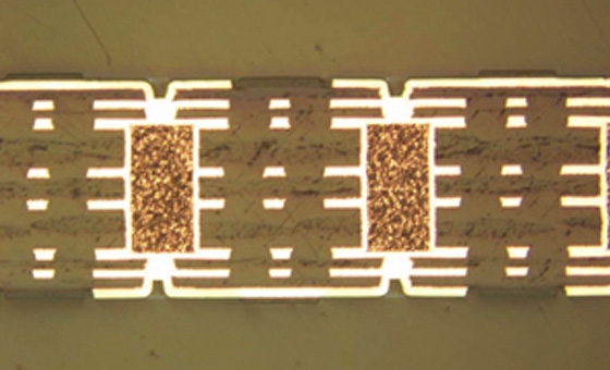
In the world of printed circuit board (PCB) manufacturing, achieving high-quality and reliable results hinges on one critical factor: PCB lamination pressure. Proper pressure control and uniform pressure application during the lamination process ensure that layers bond effectively, preventing defects and enhancing the durability of high-density interconnect (HDI) boards. In this comprehensive guide, we'll explore why pressure matters, how it impacts quality, and the best practices for avoiding lamination defects while boosting HDI reliability. Whether you're an engineer or a manufacturer, understanding these concepts is vital for producing top-tier PCBs.
What Is PCB Lamination Pressure and Why Does It Matter?
PCB lamination pressure refers to the force applied during the process of bonding multiple layers of a printed circuit board together using heat and adhesive materials like prepreg. This pressure must be carefully controlled to ensure that the layers adhere uniformly without gaps, air bubbles, or misalignment. Inadequate or uneven pressure can lead to lamination defects such as delamination, voids, or warping, which compromise the board's structural integrity and electrical performance.
Why does this matter? In modern electronics, especially with HDI designs, PCBs are becoming thinner and more complex, often featuring 8, 10, or even 20 layers. These boards must handle high-speed signals—sometimes exceeding 10 Gbps—and maintain impedance values within tight tolerances, often around ±10%. Poor lamination pressure can disrupt these characteristics, leading to signal loss or failure in critical applications like automotive systems or medical devices.
In short, mastering pressure control in PCB manufacturing is the foundation of producing reliable, high-performance boards. Let's dive deeper into the specifics of how pressure impacts the process and the techniques to optimize it.
The Role of Uniform Pressure Application in PCB Manufacturing
Uniform pressure application is the cornerstone of successful PCB lamination. When pressure is applied evenly across the entire surface of the board, it ensures consistent bonding between layers, minimizing the risk of defects. Uneven pressure, on the other hand, can create high-stress areas where layers fail to bond properly, leading to issues like voids or uneven resin flow.
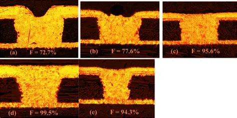
For example, in a typical multilayer PCB with a stack-up of 12 layers, uneven pressure might cause resin to pool in certain areas while leaving others under-bonded. This can result in thickness variations—sometimes as small as 0.1 mm—that affect the board's impedance, potentially shifting it outside the desired range of 50 ohms for high-speed signals. Such discrepancies can degrade signal integrity, especially in HDI designs where microvias and fine traces are common.
To achieve uniform pressure, manufacturers often rely on advanced lamination presses equipped with precise control systems. These systems monitor and adjust pressure in real-time, ensuring consistency across the board's surface. This is particularly important for larger panels, such as those measuring 18 x 24 inches, where maintaining even pressure distribution becomes more challenging.

Pressure Control Techniques for Optimal Lamination
Effective pressure control during PCB lamination involves a combination of equipment precision, process monitoring, and material selection. Here are some key techniques used in the industry to ensure optimal results:
- Advanced Lamination Presses: Modern presses come with programmable logic controllers (PLCs) that allow manufacturers to set specific pressure levels—often ranging from 200 to 500 psi—depending on the board's material and thickness. These systems can maintain pressure within ±5 psi, ensuring consistency throughout the lamination cycle.
- Temperature and Pressure Synchronization: Lamination isn't just about pressure; it's also about balancing heat. A typical process might involve heating the stack to 180°C while applying 300 psi of pressure over a 90-minute cycle. Synchronizing these parameters prevents thermal stress and ensures even curing of the prepreg material.
- Use of Cushioning Materials: To distribute pressure more evenly, manufacturers often place cushioning pads or release films between the PCB stack and the press platens. These materials help absorb minor surface irregularities, reducing the risk of localized overpressure.
- Real-Time Monitoring: Sensors embedded in lamination presses can track pressure distribution across the panel. If discrepancies are detected, the system can adjust automatically or alert operators to intervene, preventing defects before they occur.
By implementing these techniques, manufacturers can significantly reduce the likelihood of lamination defects and improve overall board quality. For HDI designs, where layer counts are high and tolerances are tight, such precision is non-negotiable.
Vectored Pressure: A Solution for Complex PCB Designs
In some advanced PCB manufacturing scenarios, particularly with HDI boards, standard uniform pressure application may not be enough. This is where vectored pressure comes into play. Vectored pressure refers to the strategic application of force in specific directions or areas of the board to address unique challenges, such as varying layer thicknesses or complex stack-ups.
For instance, in an HDI board with a mix of rigid and flexible sections, certain areas may require higher pressure to ensure proper bonding of microvias, which can be as small as 0.1 mm in diameter. Vectored pressure systems allow manufacturers to target these zones without over-pressing other parts of the board, which could lead to resin starvation or cracking.
While vectored pressure systems are more complex and costly, they are invaluable for high-reliability applications like aerospace or telecommunications, where failure is not an option. These systems often integrate with computer-aided design (CAD) software to map out pressure zones based on the board's layout, ensuring precision down to the micrometer level.
Common Lamination Defects Caused by Poor Pressure Control
Even with advanced equipment, lamination defects can occur if pressure isn't managed properly. Understanding these defects and their causes is essential for troubleshooting and prevention. Here are some of the most common issues:
- Delamination: This occurs when layers fail to bond properly due to insufficient pressure, often below 200 psi for standard FR-4 materials. Delamination can lead to electrical shorts or complete board failure, especially under thermal stress.
- Voids and Air Bubbles: Uneven pressure or improper vacuum conditions during lamination can trap air between layers, creating voids. These defects weaken the board and can cause signal interference in high-frequency applications operating above 1 GHz.
- Warping: Excessive or uneven pressure—sometimes exceeding 600 psi—can cause the board to bend or warp, making it unusable for assembly. Warping is particularly problematic for thin boards, such as those under 0.8 mm thick.
- Resin Starvation: If pressure is too high in certain areas, it can squeeze out too much resin from the prepreg, leaving insufficient material to bond the layers. This often results in weak spots prone to cracking.
By maintaining strict pressure control and adhering to process parameters, manufacturers can minimize these defects, ensuring that the final product meets industry standards for reliability and performance.
HDI Reliability and the Impact of Lamination Pressure
High-density interconnect (HDI) boards are at the forefront of modern PCB technology, enabling compact, high-performance devices like smartphones and wearables. However, their complex designs—with microvias, blind vias, and layer counts often exceeding 10—make them particularly sensitive to lamination pressure issues.
Proper pressure control is critical for HDI reliability. For example, microvias, which connect layers in HDI boards, require precise bonding to maintain electrical continuity. If pressure is uneven during lamination, the copper plating in these vias—often just 0.025 mm thick—can crack or delaminate, leading to open circuits. This is a major concern in applications requiring high signal integrity, where even a 1% failure rate is unacceptable.
Moreover, HDI boards often operate under extreme conditions, such as temperatures ranging from -40°C to 85°C in automotive environments. Poor lamination pressure can exacerbate thermal expansion mismatches between layers, causing stress fractures over time. By ensuring uniform pressure application, manufacturers can enhance the board's ability to withstand these stresses, improving long-term reliability.

Best Practices for Achieving Optimal PCB Lamination Pressure
To achieve the best results in PCB manufacturing, consider the following best practices for managing lamination pressure:
- Material Selection: Choose prepreg and core materials with compatible thermal and mechanical properties to reduce stress during lamination. For instance, using low-CTE (coefficient of thermal expansion) materials can minimize warping under pressure.
- Process Validation: Before full-scale production, conduct test runs to validate pressure settings. Use tools like pressure-sensitive films to map out distribution and identify potential problem areas.
- Equipment Maintenance: Regularly calibrate lamination presses to ensure they deliver consistent pressure. A deviation of just 10 psi can impact bonding quality in sensitive designs.
- Operator Training: Ensure that staff are well-trained in handling lamination equipment and interpreting pressure data. Human error is a common cause of defects, even with advanced systems.
Implementing these practices can make a significant difference in the quality of the final product, especially for complex designs requiring high reliability.
The Future of Pressure Control in PCB Manufacturing
As PCB technology continues to evolve, so too will the methods for controlling lamination pressure. Emerging trends include the use of artificial intelligence (AI) to predict and adjust pressure settings in real-time, based on data from thousands of previous lamination cycles. Additionally, advancements in sensor technology are enabling finer control over pressure distribution, down to the sub-millimeter level, which is crucial for next-generation HDI boards.
Another exciting development is the integration of smart materials into the lamination process. These materials can adapt to pressure variations, automatically compensating for uneven distribution and reducing the risk of defects. While still in the early stages, such innovations promise to revolutionize PCB manufacturing, making it more efficient and reliable than ever before.
Conclusion: Mastering PCB Lamination Pressure for Superior Results
In the intricate process of PCB manufacturing, lamination pressure stands out as a critical factor in determining quality and reliability. From ensuring uniform pressure application to leveraging vectored pressure for complex HDI designs, every aspect of pressure control plays a role in preventing lamination defects and enhancing performance. By adopting advanced techniques, maintaining strict process controls, and staying ahead of industry trends, manufacturers can produce boards that meet the highest standards of excellence.
Whether you're working on standard multilayer boards or cutting-edge HDI designs, understanding and optimizing PCB lamination pressure is the key to success. With the right approach, you can achieve consistent, high-quality results that power the next generation of electronic devices.