 ALLPCB


If you're an electrical engineer looking to enhance the performance and reliability of your printed circuit boards (PCBs), understanding PCB edge plating is essential. This technique, often used for shielding and improved connectivity, can significantly impact your design's electromagnetic compatibility (EMC) and thermal management. In this guide, we'll dive deep into PCB edge plating design rules, PCB edge plating specifications, PCB edge plating standards, and provide a practical PCB edge plating checklist to ensure your projects meet industry expectations and perform optimally.
Whether you're working on RF designs or high-speed digital circuits, this comprehensive resource will walk you through everything you need to know about PCB edge plating. Let's explore the fundamentals, benefits, design considerations, and best practices to help you achieve superior results.
What is PCB Edge Plating and Why Does It Matter?
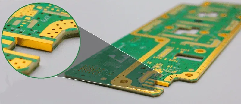
PCB edge plating, also known as board edge plating or castellation, is a manufacturing process where a conductive metal layer, typically copper, is applied along the perimeter edges of a PCB. This plating serves multiple purposes, such as providing electrical connectivity between layers, improving grounding, and offering shielding against electromagnetic interference (EMI). It is particularly critical in applications like RF designs, where signal integrity and noise reduction are paramount.
For electrical engineers, edge plating matters because it can directly affect the performance and reliability of a PCB. Without proper implementation, you risk issues like signal degradation, thermal stress, or even manufacturing defects. By adhering to specific design rules and standards, you can leverage edge plating to enhance your board's functionality while avoiding common pitfalls.
Benefits of PCB Edge Plating for Electrical Engineers
Before diving into the technical details, let's look at the key advantages of incorporating edge plating into your PCB designs:
- Improved EMC Performance: Edge plating acts as a shield, reducing EMI by creating a continuous conductive path around the board's perimeter. This is especially useful for high-frequency applications where interference can degrade performance.
- Enhanced Grounding: It provides a low-impedance path to ground, which is critical for maintaining signal integrity in high-speed circuits operating at frequencies above 1 GHz.
- Better Thermal Management: The conductive layer helps dissipate heat along the edges, preventing hotspots that could damage components or reduce lifespan.
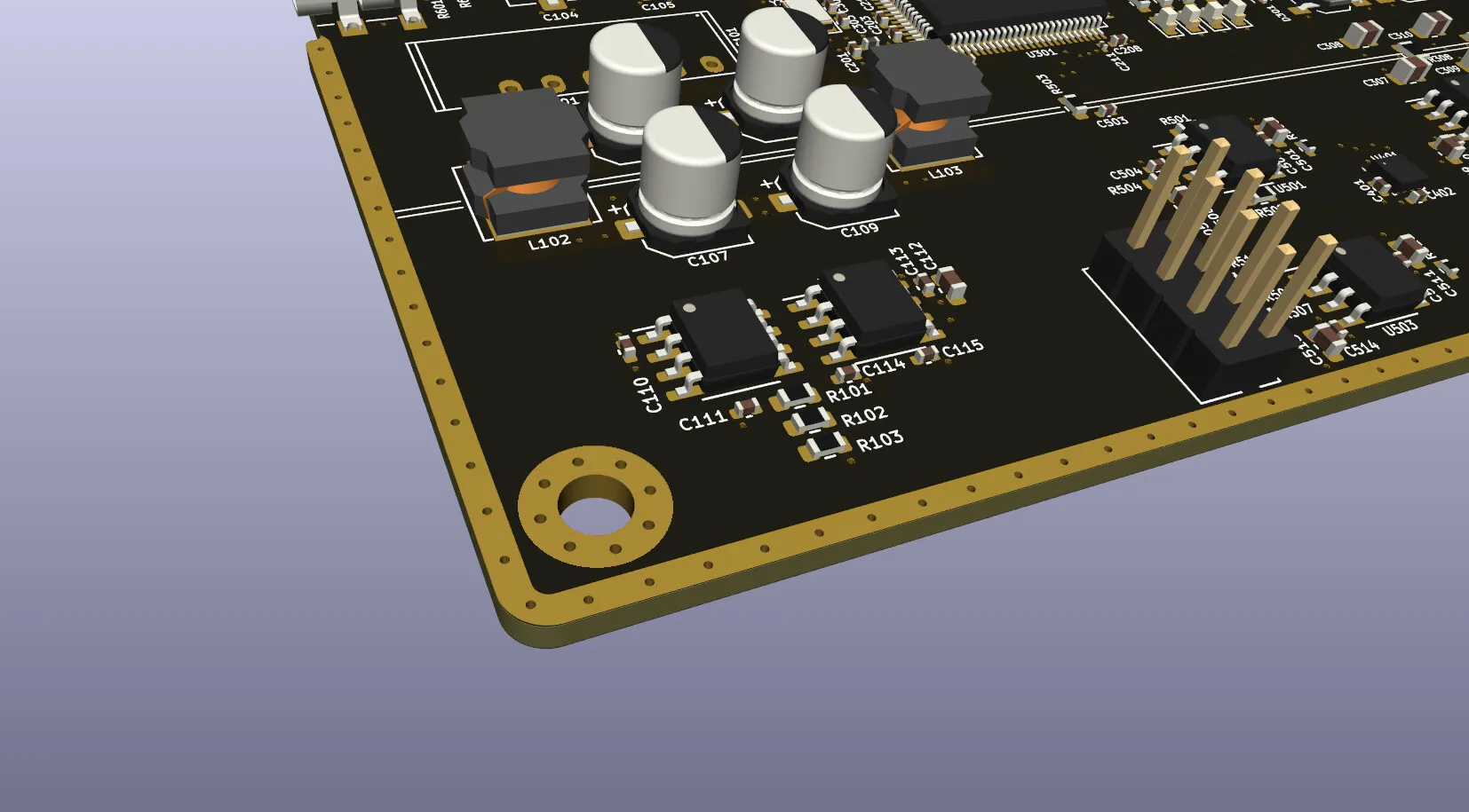
- Mechanical Strength: Edge plating adds structural integrity to the board, reducing the risk of damage during handling or assembly.
- Connectivity for Shielded Enclosures: It allows seamless contact with metal enclosures, ensuring a fully shielded environment for sensitive circuits.
Understanding these benefits helps engineers make informed decisions about when and how to use edge plating in their designs.
PCB Edge Plating Design Rules: Key Guidelines to Follow
Designing a PCB with edge plating requires careful attention to specific rules to ensure manufacturability and performance. Below are essential PCB edge plating design rules to guide your process:
1. Define Edge Plating Areas Clearly
Specify which edges of the PCB require plating in your design files. Not all edges may need plating, so clearly mark the areas in your Gerber files or design notes. Typically, plating is applied to edges where shielding or grounding is critical, such as near RF components.
2. Maintain Proper Spacing
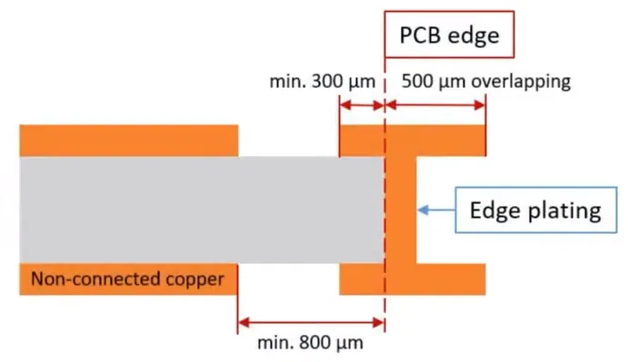
Ensure that no components, traces, or vias are placed too close to the edge where plating will be applied. A minimum clearance of 0.5 mm from the edge is often recommended to prevent shorts or damage during the plating process.
3. Consider Board Thickness
Edge plating is more effective on boards with a thickness of 1.6 mm or greater, as thinner boards may not provide enough surface area for reliable plating. Check with your manufacturing partner for their specific capabilities regarding board thickness and plating.
4. Avoid Sharp Corners
Sharp corners on the PCB edge can lead to uneven plating or stress concentration. Use rounded corners with a minimum radius of 0.3 mm to ensure uniform metal deposition and reduce the risk of cracks.
5. Specify Plating Material and Thickness
Commonly, copper is used for edge plating with a thickness ranging from 25 to 50 micrometers, followed by a protective finish like ENIG (Electroless Nickel Immersion Gold). Clearly define these parameters in your design to meet electrical and durability requirements.
PCB Edge Plating Specifications: Meeting Industry Requirements
When incorporating edge plating, adhering to PCB edge plating specifications ensures compatibility with manufacturing processes and end-use applications. Here are key specifications to consider:
1. Conductive Layer Continuity
The plated edge must provide a continuous conductive path with no breaks or gaps. Discontinuities can compromise shielding effectiveness and grounding. Ensure your design allows for uniform plating across the specified edges.
2. Surface Finish Compatibility
The edge plating should match the board’s surface finish to prevent corrosion or connectivity issues. For instance, if your PCB uses an ENIG finish, the edge plating should also have a compatible nickel and gold layer to maintain consistency.
3. Electrical Resistance
The resistance of the plated edge should be low, typically less than 1 milliohm per square centimeter, to ensure effective grounding and minimal signal loss. Test this parameter during prototyping to validate your design.
4. Manufacturing Tolerances
Edge plating often requires tighter tolerances than standard PCB features. A typical tolerance for edge plating alignment is ±0.1 mm. Work closely with your manufacturer to confirm their capabilities and adjust your design accordingly.
By meeting these specifications, you can avoid costly redesigns and ensure your PCB performs as intended in its final application.
PCB Edge Plating Standards: Industry Benchmarks to Follow
Compliance with industry PCB edge plating standards is crucial for producing high-quality boards that meet performance and reliability expectations. Below are some widely recognized standards relevant to edge plating:
1. IPC-6012: Qualification and Performance Specification for Rigid PCBs
This standard outlines requirements for PCB manufacturing, including edge plating. It specifies criteria for plating thickness, adhesion, and continuity to ensure the plated edges meet electrical and mechanical performance needs.
2. IPC-A-610: Acceptability of Electronic Assemblies
While primarily focused on assembly, this standard includes guidelines for edge plating as part of the overall board quality. It defines acceptable visual and functional criteria for plated edges, such as the absence of voids or delamination.
3. IPC-2221: Generic Standard on Printed Board Design
This standard provides design guidelines for PCBs, including recommendations for edge features like plating. It emphasizes proper spacing, material selection, and structural considerations to support effective edge plating.
Following these standards not only ensures quality but also facilitates communication with manufacturers, reducing the likelihood of errors during production.
PCB Edge Plating Checklist: A Practical Tool for Engineers
To simplify the design and implementation process, use this PCB edge plating checklist as a step-by-step guide:
- Identify Plating Requirements: Determine which edges need plating based on shielding, grounding, or connectivity needs.
- Review Design Files: Ensure your Gerber files and documentation clearly indicate plating areas and specifications.
- Check Clearances: Verify that components and traces are at least 0.5 mm away from plated edges to avoid interference.
- Specify Materials: Define the plating material (e.g., copper) and finish (e.g., ENIG) in your design notes.
- Confirm Board Thickness: Ensure the PCB thickness supports edge plating, ideally 1.6 mm or more.
- Design Rounded Corners: Use a minimum corner radius of 0.3 mm to prevent stress and uneven plating.
- Validate with Manufacturer: Discuss tolerances, capabilities, and any additional costs with your manufacturing partner before finalizing the design.
- Test Prototypes: Measure resistance and inspect continuity of plated edges during prototyping to confirm performance.
This checklist serves as a quick reference to streamline your workflow and minimize errors in the design phase.
Common Challenges in PCB Edge Plating and How to Overcome Them
While edge plating offers numerous benefits, it also comes with potential challenges. Here are some common issues and solutions:
1. Uneven Plating
Uneven metal deposition can lead to poor conductivity or weak shielding. To avoid this, ensure your design avoids sharp corners and complex geometries at the edges. Work with your manufacturer to optimize the plating process parameters.
2. Increased Manufacturing Costs
Edge plating is a specialized process that can add to production costs. To manage expenses, limit plating to only the necessary edges and discuss cost-effective options with your manufacturer.
3. Risk of Shorts
If components or traces are too close to the plated edge, shorts can occur. Adhere to the recommended clearance of 0.5 mm or more and perform thorough design reviews to catch potential issues early.
By anticipating these challenges and planning accordingly, you can ensure a smoother design and manufacturing process.
Applications of PCB Edge Plating in Modern Electronics
Edge plating is widely used across various industries due to its ability to enhance PCB performance. Some notable applications include:
- RF and Wireless Devices: Edge plating provides critical EMI shielding for devices like smartphones and IoT modules operating at frequencies up to 5 GHz.
- Automotive Electronics: In automotive systems, edge plating ensures reliable grounding and thermal management for control units and sensors.
- Medical Equipment: High-precision medical devices use edge plating to maintain signal integrity and protect against interference in sensitive environments.
- Aerospace Systems: Edge plating supports robust shielding and durability in harsh conditions faced by aerospace electronics.
Understanding these applications can help you determine if edge plating is the right choice for your specific project.
Final Thoughts on Mastering PCB Edge Plating
PCB edge plating is a powerful technique for electrical engineers looking to optimize their designs for EMC, grounding, and thermal performance. By following the PCB edge plating design rules, meeting PCB edge plating specifications, adhering to PCB edge plating standards, and using a practical PCB edge plating checklist, you can achieve reliable and high-performing boards tailored to your application needs.
Remember to collaborate closely with your manufacturing partner to align on capabilities and tolerances, and always validate your design through prototyping and testing. With careful planning and attention to detail, edge plating can elevate the quality and functionality of your PCB projects.


