 ALLPCB


In the fast-paced world of electronics, precision and efficiency in PCB manufacturing are critical. If you're an engineer looking to understand the PCB direct imaging process or seeking a clear LDI workflow, you're in the right place. This guide breaks down the direct imaging procedure into simple, actionable steps, helping you navigate the PCB production process with confidence. Whether you're designing complex multilayer boards or optimizing production timelines, mastering the PCB manufacturing steps involving direct imaging can significantly boost your project's success.
In this comprehensive blog, we'll walk through every stage of the PCB direct imaging workflow, explain how Laser Direct Imaging (LDI) transforms traditional methods, and provide practical insights for engineers. Let’s dive into the details of this cutting-edge technology and explore how it streamlines the PCB production process.
What is PCB Direct Imaging and Why Does It Matter?
PCB direct imaging, often referred to as Laser Direct Imaging (LDI), is a modern technique used in the PCB manufacturing steps to transfer circuit patterns onto a board's photosensitive layer. Unlike traditional methods that rely on physical photomasks or film, LDI uses a computer-controlled laser to directly expose the pattern onto the board. This results in higher precision, especially for fine lines and ultra-fine traces down to 25 micrometers or smaller, which are common in high-density interconnect (HDI) designs.
Why is this important for engineers? The direct imaging procedure eliminates alignment errors, reduces production time, and supports the creation of complex designs needed for modern devices like 5G hardware or compact IoT gadgets. By understanding the LDI workflow, you can ensure your designs are manufactured with accuracy, minimizing costly revisions and delays in the PCB production process.
Key Benefits of Laser Direct Imaging in PCB Manufacturing
Before we explore the step-by-step PCB direct imaging process, let’s highlight why LDI is a game-changer in the industry:
- Precision: Achieves line widths and spacing as small as 1 mil (25.4 micrometers), ideal for HDI and microvia boards.
- Speed: Eliminates the need for creating and aligning photomasks, cutting down setup time by up to 50% in some cases.
- Flexibility: Allows quick design changes since patterns are digitally controlled, reducing turnaround time for prototypes.
- Cost-Effectiveness: Reduces material waste and labor costs associated with traditional film-based imaging.
Step-by-Step Guide to the PCB Direct Imaging Workflow
Now, let’s break down the LDI workflow into clear, actionable steps. This guide is tailored for engineers who want to understand how the direct imaging procedure fits into the broader PCB manufacturing steps.
Step 1: Design Preparation and Data Conversion
The PCB direct imaging process begins with your design files. These are typically created in CAD software and exported in standard formats like Gerber or ODB++. The data must be converted into a format compatible with the LDI system, ensuring that every trace, pad, and via is accurately represented.
During this stage, the system checks for design rule violations, such as spacing issues or incomplete traces. Engineers should ensure that impedance values—for instance, maintaining 50 ohms for high-speed signals—are accounted for in the design to avoid signal integrity issues during manufacturing.
Tip for Engineers: Double-check your layer stack-up and confirm that critical dimensions are within the LDI system’s capability, typically down to 25 micrometers for fine traces.
Step 2: Board Preparation and Photosensitive Coating
Once the design data is ready, the physical PCB substrate is prepared. The board, often made of FR-4 or other materials, is cleaned to remove contaminants. A photosensitive resist layer, also known as photoresist, is then applied to the surface. This layer reacts to the laser during the direct imaging procedure, forming the circuit pattern.
The quality of this coating is critical. Any unevenness or defects can lead to imaging errors, affecting the final board’s performance. The thickness of the photoresist is usually between 20 to 50 micrometers, depending on the design requirements.
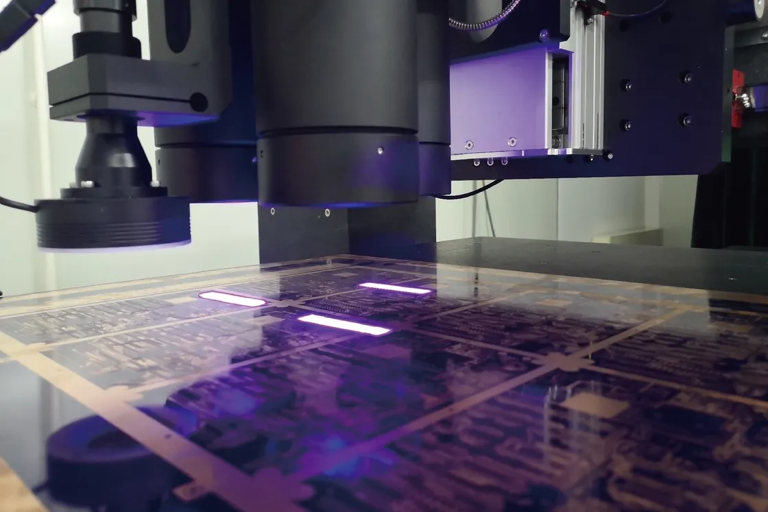
Step 3: Laser Direct Imaging Exposure
This is the heart of the PCB direct imaging process. The prepared board is placed in the LDI machine, where a computer-controlled laser beam directly exposes the photosensitive layer based on the design data. The laser, often operating at wavelengths around 355 nanometers (UV range), selectively hardens or removes the photoresist to create the circuit pattern.
The exposure process is incredibly precise, with resolutions supporting trace widths as narrow as 1 mil. This step in the LDI workflow can handle complex multilayer boards and high-speed designs, ensuring signal speeds up to several gigahertz are maintained without interference.
Tip for Engineers: Ensure your design accounts for the laser’s spot size and energy settings to avoid overexposure or underexposure of the resist layer.
Step 4: Development of the Exposed Pattern
After exposure, the board undergoes a development process where unexposed areas of the photoresist are washed away using a chemical solution. This reveals the copper layer beneath in the desired pattern, ready for etching. The development time and chemical concentration must be carefully controlled to prevent under- or over-development, which could distort traces.
For high-precision boards, such as those used in 5G applications, this step ensures that microvias with diameters as small as 50 micrometers are accurately formed.
Step 5: Etching and Resist Removal
With the pattern developed, the exposed copper is etched away using an acidic solution, leaving only the desired circuit traces protected by the hardened photoresist. Once etching is complete, the remaining photoresist is stripped off, revealing the final copper pattern on the board.
This step is crucial in the PCB manufacturing steps as it directly impacts the board’s electrical performance. For instance, maintaining consistent trace widths ensures impedance control, critical for high-frequency signals operating at 2.4 GHz or higher.
Step 6: Inspection and Quality Control
Quality control is a non-negotiable part of the PCB production process. After imaging and etching, the board is inspected using automated optical inspection (AOI) systems to detect defects like broken traces or shorts. For critical applications, electrical testing may also be conducted to verify impedance values, ensuring they match the design specifications (e.g., 50 ohms for RF signals).
LDI’s precision reduces defects, but inspection ensures that any anomalies are caught early, preventing costly rework later in the assembly process.
Step 7: Proceeding to Further Manufacturing Stages
Once the imaging and initial patterning are complete, the board moves to additional PCB manufacturing steps like drilling, plating, solder mask application, and silkscreen printing. The accuracy of the direct imaging procedure ensures that subsequent layers align perfectly, especially for multilayer boards with up to 20 layers or more.
Engineers should note that the LDI workflow integrates seamlessly with these later stages, reducing cumulative errors and supporting faster production cycles.
Challenges in the PCB Direct Imaging Process and How to Overcome Them
While the PCB direct imaging process offers numerous advantages, it’s not without challenges. Here are a few common issues and solutions:
- High Initial Equipment Cost: LDI systems are expensive to acquire. Partnering with a reliable manufacturing service can offset this by providing access to advanced technology without the upfront investment.
- Complex Data Management: Handling large design files for LDI requires robust software. Ensure your design tools are optimized for high-resolution outputs to avoid data conversion errors.
- Material Sensitivity: Photoresist materials must be compatible with the laser wavelength. Work closely with your manufacturing team to select the right materials for your specific design needs.
How LDI Enhances Specific PCB Applications
The LDI workflow is particularly beneficial for certain types of PCB designs. Here’s how it impacts specific applications:
- High-Density Interconnect (HDI) Boards: LDI supports microvias and fine traces, essential for compact devices like smartphones, with via diameters as small as 50 micrometers.
- Flexible PCBs: The precision of LDI ensures accurate imaging on thin, flexible substrates, maintaining signal integrity for wearable tech.
- 5G and High-Speed Designs: With controlled impedance and minimal signal loss, LDI is ideal for boards handling frequencies above 2 GHz.
Comparing LDI to Traditional Imaging Methods
To fully appreciate the value of the direct imaging procedure, let’s compare it to traditional photomask-based imaging:
| Aspect | Laser Direct Imaging (LDI) | Traditional Photomask Imaging |
|---|---|---|
| Precision | Supports traces down to 25 micrometers | Limited to around 50 micrometers |
| Setup Time | Minimal, as it’s digitally controlled | Longer due to photomask creation |
| Cost for Small Runs | More cost-effective due to no mask costs | Higher due to mask production |
This comparison shows why LDI is becoming the preferred choice in the PCB production process, especially for prototypes and small-batch production.
Tips for Engineers to Optimize the LDI Workflow
As an engineer, you play a key role in ensuring the PCB direct imaging process runs smoothly. Here are practical tips to optimize your designs for LDI:
- Design with LDI limitations in mind, such as minimum trace widths and spacing (typically 1 mil or 25 micrometers).
- Use high-resolution design files to prevent data loss during conversion for the LDI system.
- Collaborate with your manufacturing partner early to confirm material compatibility and laser settings.
- Include test points in your design to facilitate electrical testing post-imaging, ensuring impedance matches (e.g., 50 ohms for high-speed signals).
Conclusion: Streamlining PCB Production with Direct Imaging
The PCB direct imaging workflow is revolutionizing the way engineers and manufacturers approach the PCB production process. By leveraging the precision and efficiency of Laser Direct Imaging, you can achieve unparalleled accuracy for complex designs, reduce production timelines, and minimize errors in the PCB manufacturing steps. Whether you’re working on HDI boards, flexible circuits, or high-speed applications, understanding the LDI workflow equips you with the knowledge to optimize your projects.
At ALLPCB, we’re committed to supporting engineers with cutting-edge solutions in the direct imaging procedure. By integrating advanced technologies like LDI into our processes, we ensure that your designs are brought to life with the highest quality and speed. Explore how this technology can transform your next project and take your PCB manufacturing to the next level.


