 ALLPCB


If you're diving into DIY PCB design and wondering how to improve signal quality in your home-fabricated boards, PCB back drilling might be the technique you need. This process helps reduce signal loss in high-speed circuits by removing unused portions of vias that can interfere with signal integrity. In this guide, we'll explore PCB back drilling basics, its importance in DIY PCB design, and simple back drilling methods for home PCB fabrication. Whether you're a hobbyist or an aspiring engineer, you'll find actionable tips to enhance your projects and minimize signal loss.
What Is PCB Back Drilling and Why Does It Matter?
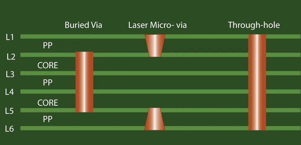
PCB back drilling is a manufacturing technique used to remove the unused portion of a via—known as a stub—in a multilayer printed circuit board (PCB). Vias are small holes that connect different layers of a PCB, allowing electrical signals to pass through. However, in high-speed or high-frequency designs, the unused part of a via can act like an antenna, causing signal reflections and loss. Back drilling addresses this by drilling out the stub, leaving only the necessary conductive path.
For DIY enthusiasts working on home PCB fabrication, signal loss reduction is critical, especially if you're designing circuits for fast data transfer or sensitive applications like RF communication. Without proper signal integrity, your project might suffer from noise, delays, or even complete failure. Back drilling is a powerful way to tackle these issues, and while it’s often associated with professional manufacturing, there are simplified approaches you can adapt for DIY PCB design.
Understanding Signal Loss in PCBs
Before we dive deeper into back drilling, let’s break down why signal loss happens in PCBs. When a signal travels through a via in a multilayer board, any unused portion of that via (the stub) can create a resonance effect. This resonance causes signal reflections, where part of the signal bounces back instead of continuing forward. The result? Degraded signal quality, increased noise, and potential data errors.
In high-speed designs, where signals can operate at frequencies above 1 GHz, even a small stub measuring 0.5 mm can cause significant issues. For instance, a stub can introduce a signal delay or impedance mismatch, disrupting the intended 50-ohm impedance often used in high-frequency circuits. This is why signal loss reduction is a top priority for engineers and hobbyists alike.
In DIY PCB design, you might not always work with multilayer boards or high-speed signals. However, as projects become more complex—think microcontrollers, USB interfaces, or wireless modules—understanding and mitigating signal loss becomes essential, even at home.
The Basics of PCB Back Drilling
Back drilling involves using a drill to remove the conductive material from the unused portion of a via after the initial plating process. In professional setups, this is done with precision machines that can control the depth of the drill to avoid damaging the active layers of the PCB. The goal is to eliminate the stub while maintaining the integrity of the via’s functional part.
For example, in a 6-layer PCB, a via might connect layers 1 and 2 but extend through layers 3 to 6 as a stub. Back drilling removes the conductive material from layers 3 to 6, reducing the stub’s impact on signal integrity. The result is a cleaner signal path with less interference.
While professional back drilling uses advanced equipment, DIY hobbyists can approximate this technique with careful planning and manual tools. We’ll cover these methods later, tailored for home PCB fabrication.
Benefits of Back Drilling for Signal Loss Reduction
Back drilling offers several advantages, especially for high-speed or high-frequency designs. Here are the key benefits that make it worth considering for your DIY projects:
- Improved Signal Integrity: By removing via stubs, back drilling minimizes signal reflections and ensures that signals travel smoothly through the intended path.
- Reduced Noise: Stubs can introduce electromagnetic interference (EMI). Back drilling cuts down on this noise, leading to cleaner performance.
- Better Impedance Control: Stubs can disrupt the impedance of a signal path. Removing them helps maintain consistent impedance, such as the standard 50 ohms used in many high-speed designs.
- Enhanced Performance for High-Speed Signals: If your DIY project involves data rates above 1 Gbps, back drilling can significantly improve reliability.
Even if you’re not working on cutting-edge designs, these benefits can future-proof your projects as you scale up to more complex circuits.
Challenges of Back Drilling in DIY PCB Design
While back drilling is highly effective, it comes with challenges, especially for home PCB fabrication. Professional setups use computer-controlled drilling machines with depth accuracy down to 0.1 mm. At home, achieving this precision is difficult without specialized tools. Here are some hurdles you might face:
- Lack of Precision Equipment: Standard drills used in DIY setups may not offer the depth control needed for accurate back drilling.
- Risk of Damage: Drilling too deep can harm the functional layers of your PCB, rendering it unusable.
- Time-Intensive Process: Manual back drilling, even on a small scale, requires patience and careful execution.
Despite these challenges, there are ways to adapt back drilling for DIY projects. Let’s explore how you can implement simple back drilling techniques at home.
Simple Back Drilling Techniques for Home PCB Fabrication
For hobbyists, back drilling doesn’t have to be a complex or expensive process. While you may not achieve the same precision as industrial methods, you can still reduce signal loss in your DIY PCB design with these practical steps. Always prioritize safety by wearing protective gear and working in a well-ventilated space.
Step 1: Plan Your PCB Layout Carefully
Before you even think about drilling, design your PCB layout to minimize the need for long vias. Use software tools to route signals on the top or bottom layers whenever possible, reducing the number of vias that pass through multiple layers. If a via must go through several layers, note its location and plan which part needs to be drilled out.
Step 2: Use a Manual Drill with Depth Control
For home PCB fabrication, a small hand drill or a drill press with an adjustable depth stop can work for back drilling. Set the depth carefully to avoid drilling into active layers. For a 1.6 mm thick board, if you only need the via to connect the top two layers (about 0.4 mm deep), set your drill depth to start just below this point and remove the stub from the remaining thickness.
Step 3: Test on a Scrap Board First
Practice on a scrap PCB before working on your actual project. This helps you get a feel for the drill’s depth and speed. Mark the via locations with a fine-tip marker to guide your drilling, and use a magnifying glass to inspect the results.
Step 4: Inspect and Clean After Drilling
After back drilling, check the via to ensure no debris or burrs remain. Use a small brush or compressed air to clean the area. Test the board with a multimeter to confirm that the active layers of the via are still connected and functional.
While this manual approach won’t match the precision of professional back drilling, it can still help with signal loss reduction in less critical high-speed projects. For more demanding designs, consider partnering with a fabrication service that offers back drilling as a standard feature.
Alternative Signal Loss Reduction Tips for DIY PCB Design
If back drilling feels too complex for your current setup, there are other ways to minimize signal loss in your DIY projects. These methods complement or even replace the need for back drilling in some cases.
Optimize Via Placement and Size
Keep vias as short as possible by routing signals on outer layers. Also, use the smallest via drill size that your design and fabrication process can handle. Smaller vias (down to 0.2 mm in some cases) reduce the stub effect and lower parasitic capacitance, which can degrade signals.
Use Blind or Buried Vias
If your design software and fabrication process allow, consider blind or buried vias. These connect only the necessary layers without creating a stub, eliminating the need for back drilling. Note that this may require more advanced tools or services beyond basic home PCB fabrication.
Maintain Consistent Trace Widths
Signal integrity depends on consistent impedance. Ensure that your trace widths and spacing match the impedance requirements of your design, such as 50 ohms for high-frequency signals. Use online calculators to determine the correct dimensions for your board’s material and thickness.
When to Consider Professional Fabrication
For complex multilayer boards or projects with signals above 2.5 Gbps, professional fabrication might be the better choice. Many services offer back drilling as a standard option, ensuring precision and reliability that’s hard to achieve at home. If your DIY project is a stepping stone to a larger product, investing in professional help can save time and prevent costly mistakes.
Conclusion: Elevate Your DIY PCB Projects with Back Drilling
PCB back drilling is a valuable technique for reducing signal loss and improving performance in high-speed designs. While it’s rooted in professional manufacturing, hobbyists can adapt simple back drilling methods for home PCB fabrication with careful planning and the right tools. By understanding PCB back drilling basics and applying signal loss reduction strategies, you can take your DIY PCB design skills to the next level.
Start small by practicing on scrap boards, and don’t hesitate to explore alternative methods like optimizing via placement or maintaining impedance control. With these tips, you’ll be well on your way to creating cleaner, more reliable circuits for your projects. Keep experimenting, and watch your designs improve with every board you build.


