 ALLPCB


If you're looking to maximize your PCB production efficiency, the secret lies in panel utilization. By optimizing how you arrange multiple PCBs on a single panel, you can reduce costs, increase production yield, and streamline the manufacturing process. In this blog, we'll dive deep into proven strategies and tools for getting the most out of every board, focusing on PCB panel layout software, PCB panelization cost analysis, PCB manufacturing process optimization, increasing PCB production yield, and PCB design for manufacturability.
Whether you're an engineer aiming to cut expenses or a manufacturer seeking higher output, this guide will walk you through actionable tips and techniques to improve your panel designs. Let's explore how small changes in layout and planning can lead to big savings and better results.
What Is PCB Panelization and Why Does It Matter?
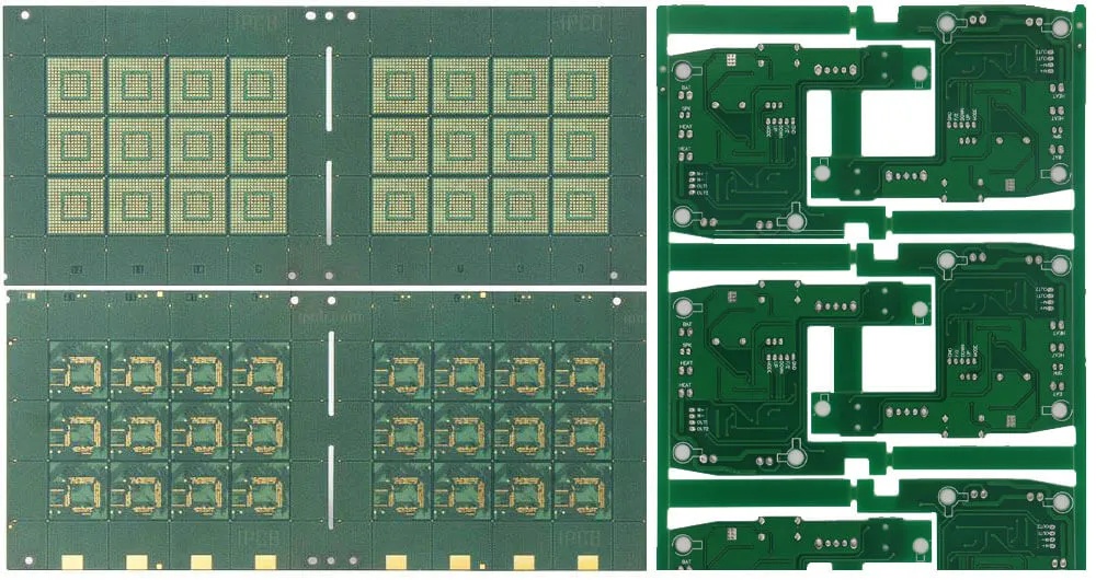
PCB panelization is the process of arranging multiple printed circuit boards (PCBs) on a single larger panel for manufacturing. This approach allows manufacturers to produce several boards at once, reducing handling time and material waste. Efficient panelization directly impacts cost, speed, and quality in PCB production.
Imagine you're producing 100 small PCBs. Fabricating each one individually would take significant time and resources. By grouping them onto a single panel—say, 10 boards per panel—you cut the number of fabrication cycles down to 10. This not only speeds up production but also lowers costs per unit. However, poor panel utilization can lead to wasted space, higher material costs, and even damage during assembly if boards are not arranged properly.
Optimizing panel utilization is key to addressing challenges like rising material costs and tight production schedules. In the sections below, we'll break down how to achieve this through smart design, software tools, and cost analysis.
Key Factors in PCB Panel Utilization for Maximum Yield
To squeeze more PCBs onto every board, you need to focus on several critical factors during the design and planning stages. Here are the main elements that influence panel utilization and production yield:
1. Board Size and Shape Optimization
The size and shape of individual PCBs play a huge role in how many can fit on a panel. Standard panel sizes in the industry are often 18 x 24 inches or 21 x 24 inches, though this varies by manufacturer. If your PCB dimensions don't align well with these panel sizes, you may end up with unused space.
For example, if your PCB is 2 x 3 inches, arranging them in a grid on an 18 x 24-inch panel might allow for 48 boards (6 rows by 8 columns) with minimal waste. However, irregular shapes or larger boards might reduce this number. To counter this, consider rotating boards or using a mix of orientations to fill gaps. This technique, often called "tessellation," can increase panel utilization by up to 15-20% in some cases.
2. Spacing and Clearances
Proper spacing between boards is essential for manufacturing processes like cutting and assembly. Most manufacturers require a minimum clearance of 0.1 to 0.2 inches (2.5 to 5 mm) between boards to allow for V-cuts or routing. Additionally, you need to account for edge clearances—typically 0.5 inches (12.7 mm) from the panel border—to ensure safe handling and tooling.
Balancing tight spacing with these requirements can help fit more boards without risking damage during separation. Overcrowding can lead to issues like tool breakage or board cracking, which reduces yield.
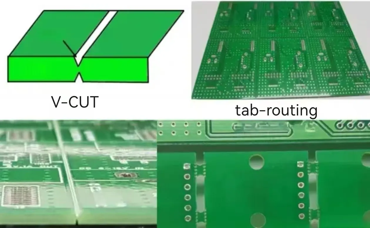
3. Panelization Methods: V-Cut vs. Tab Routing
The method you choose to separate individual PCBs from the panel also affects utilization. V-Cut is a common technique that uses straight cuts to create grooves, making it ideal for rectangular boards. It allows for tight spacing but limits design flexibility. Tab routing, on the other hand, uses small breakable tabs to hold irregular-shaped boards in place, offering more layout options at the cost of slightly more space per board.
Choosing the right method based on your board design can save up to 10% of panel space, directly impacting how many PCBs you can produce per run.
PCB Panel Layout Software: Tools to Boost Efficiency
Manually arranging PCBs on a panel can be time-consuming and prone to errors. This is where PCB panel layout software comes in. These tools automate the process, helping you achieve optimal layouts with minimal waste. Here's how software can transform your panelization efforts:
Modern design tools often include panelization features that allow you to input panel dimensions, board sizes, and spacing requirements. The software then calculates the best arrangement to maximize the number of boards per panel. Some programs even suggest rotations or mixed orientations to fill gaps, increasing utilization rates by as much as 25% compared to manual methods.
Additionally, these tools can simulate manufacturing constraints, such as tooling holes or fiducial marks, ensuring your design is ready for production. By integrating PCB design for manufacturability principles into the software, you avoid costly redesigns and delays. Look for software with features like drag-and-drop interfaces, real-time cost estimators, and compatibility with common file formats like Gerber.
Using PCB panel layout software not only saves time but also provides data for PCB panelization cost analysis, which we'll explore next.
PCB Panelization Cost Analysis: Save Money with Smart Planning
Effective panel utilization isn't just about fitting more boards—it's also about reducing costs. A thorough PCB panelization cost analysis can reveal hidden savings in material usage, labor, and production time. Here's how to approach it:
1. Material Costs
The cost of raw materials, like FR-4 substrate, is a major factor in PCB production. If your panel utilization rate is low—say, only 60% of the panel is used—you're paying for unused material. By increasing utilization to 85% or higher through optimized layouts, you can significantly cut material expenses. For instance, on a $50 panel, improving utilization from 60% to 85% could save $12.50 per panel in material costs alone.
2. Manufacturing Time
More boards per panel mean fewer panels to process, which reduces machine time and labor costs. If a single panel takes 30 minutes to fabricate and assemble, producing 10 panels instead of 15 saves 2.5 hours of production time. At an hourly rate of $100, that's a $250 saving per batch.
3. Yield Losses
Poor panel designs can lead to damaged boards during separation or assembly, lowering yield. A well-planned layout with proper clearances and separation methods can boost yield from, say, 90% to 98%, reducing waste and rework costs.
By regularly conducting a PCB panelization cost analysis, you can identify inefficiencies and adjust your designs for maximum savings. Pairing this with software tools makes the process even easier, as many programs provide cost estimates based on your layout.
PCB Manufacturing Process Optimization: Streamline Production
Beyond panel layout, optimizing the entire PCB manufacturing process is crucial for squeezing more value from each board. Here are key strategies to focus on:
1. Standardize Panel Sizes
Work with standard panel sizes to avoid custom fabrication, which often comes with higher costs and longer lead times. Aligning your designs with commonly used dimensions (like 18 x 24 inches) ensures better compatibility with equipment and reduces setup time.
2. Minimize Layer Count Variations
If your panel contains boards with different layer counts (e.g., some 2-layer and some 4-layer), it complicates manufacturing. Grouping similar boards on the same panel simplifies the process, cutting down on setup changes and potential errors.
3. Plan for Assembly
Consider how your panel will be handled during assembly. For example, adding tooling holes or fiducial marks helps automated machines align components accurately, reducing errors and speeding up production. Proper panel design can cut assembly time by 10-15% in high-volume runs.
By focusing on PCB manufacturing process optimization, you create a smoother workflow that complements your panel utilization efforts, ultimately increasing PCB production yield.
Increasing PCB Production Yield with Smart Design
Yield—the percentage of usable boards produced per run—is a critical metric in PCB manufacturing. Low yield means more waste, higher costs, and delays. Here’s how to increase PCB production yield through panel utilization:
First, ensure uniform spacing and clearances to prevent damage during cutting. A board placed too close to the edge or another board risks cracking, which can lower yield by 5-10%. Second, use high-quality separation methods like V-Cut for straight-edged boards to minimize stress on the material.
Another tip is to avoid overcomplicating panel designs. Mixing too many board types or orientations can lead to errors during fabrication or assembly. Stick to consistent layouts where possible to maintain high yield rates, ideally above 95%.
Finally, test your panel design with a small batch before full-scale production. This helps identify issues like misalignment or weak tabs that could affect yield, saving you from costly mistakes later.
PCB Design for Manufacturability: Build with Production in Mind
One of the most effective ways to improve panel utilization is to embrace PCB design for manufacturability (DFM) principles from the start. DFM focuses on creating designs that are easy and cost-effective to produce. Here's how it ties into panelization:
Simplify Board Shapes: Complex shapes with curves or cutouts can waste space on a panel. Whenever possible, stick to rectangular or simple geometries to maximize how many boards fit.
Account for Tolerances: Manufacturing equipment has limits on precision. Designing with tolerances in mind—such as a minimum trace width of 6 mils (0.15 mm) for standard processes—ensures your boards can be produced without issues, reducing scrap rates.
Communicate with Manufacturers: Early collaboration with your manufacturing partner can reveal specific constraints or recommendations for panel design. For instance, they might suggest a particular panel size or spacing to align with their equipment, boosting efficiency.
By prioritizing PCB design for manufacturability, you set the stage for better panel utilization and overall production success.
Practical Tips to Get Started Today
Ready to squeeze more PCBs onto every board? Here are some quick, actionable tips to implement right away:
- Start Small: Experiment with panel layouts on a small scale to test utilization rates before committing to large runs.
- Use Software: Leverage PCB panel layout software to automate and optimize your designs, saving time and reducing errors.
- Analyze Costs: Regularly perform a PCB panelization cost analysis to track savings and identify areas for improvement.
- Prioritize Yield: Focus on increasing PCB production yield by refining spacing, separation methods, and design consistency.
- Think Ahead: Incorporate PCB design for manufacturability principles early in the design process to avoid costly redesigns.
Conclusion: Unlock the Power of Panel Utilization
Maximizing panel utilization is a game-changer for PCB production. By carefully planning layouts, using the right tools, and focusing on PCB manufacturing process optimization, you can fit more boards onto every panel, reduce costs, and boost efficiency. Whether you're diving into PCB panel layout software or conducting a detailed PCB panelization cost analysis, each step brings you closer to higher yields and better results.
Start applying these panel utilization secrets today to see tangible improvements in your production process. With smart design and strategic planning, you'll not only squeeze more PCBs onto every board but also build a more sustainable and profitable operation.


