ALLPCB


When designing printed circuit boards (PCBs) for manufacturing, one critical aspect often overlooked is the placement of breakaway tabs. These small connectors hold individual boards together in a panel during fabrication and assembly, allowing for easy separation later. However, if not placed thoughtfully, breakaway tabs can introduce significant stress during depanelization, risking damage to the PCB or its components. So, how can you optimize breakaway tab placement to minimize stress? The key lies in strategic positioning, understanding stress distribution, and leveraging design tools for analysis. In this comprehensive guide, we’ll dive deep into techniques for breakaway tab stress analysis, PCB depanelization stress reduction, and more, ensuring your boards remain intact and functional.
Why Breakaway Tab Placement Matters in PCB Design
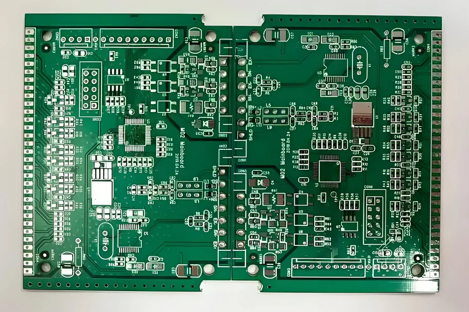
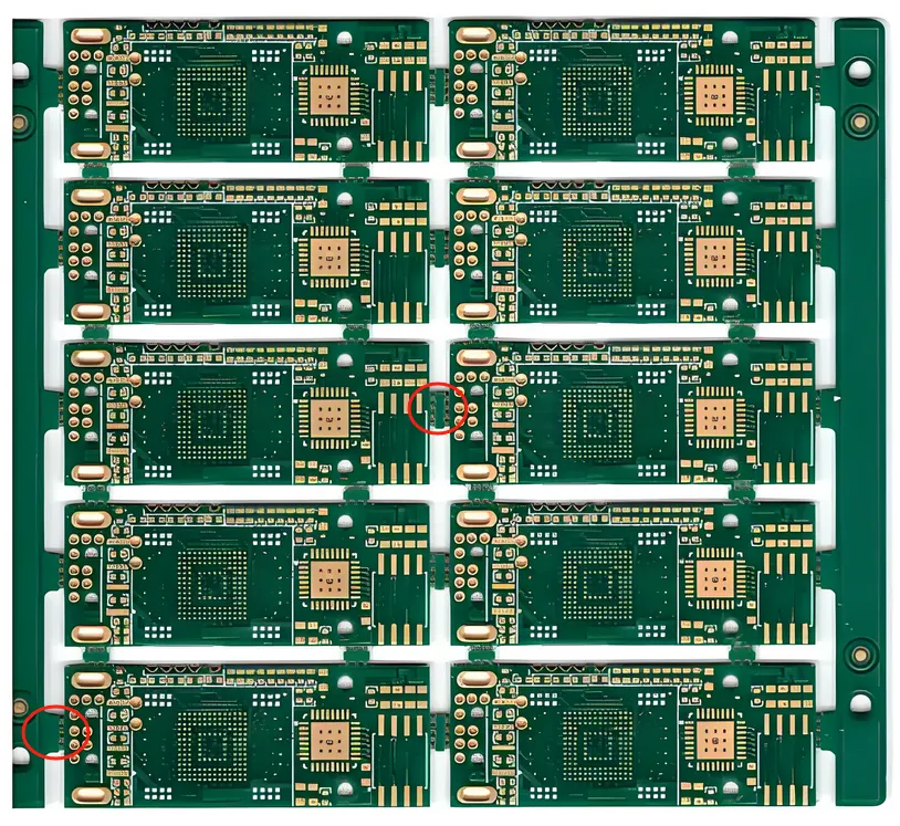
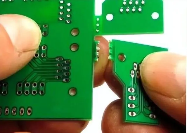
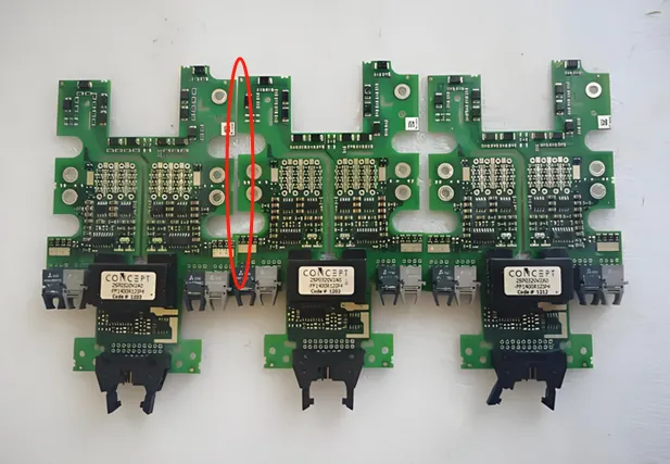
Breakaway tabs, sometimes called mouse bites, are essential for PCB panelization, a process where multiple boards are manufactured as a single panel for efficiency. These tabs keep the boards connected during production but must break cleanly during depanelization without causing cracks, delamination, or component failure. Poorly placed tabs can lead to uneven stress distribution, causing board flex or damage to sensitive areas. By optimizing their placement, you can achieve minimizing board flex during depaneling and ensure a smoother manufacturing process.
Understanding Stress in PCB Depanelization
During depanelization, the force applied to separate boards can create mechanical stress, especially near the breakaway tabs. This stress can propagate through the board, potentially damaging traces, solder joints, or components. Factors contributing to stress include:
- Tab Location: Tabs placed too close to critical components or thin board sections can concentrate stress in vulnerable areas.
- Tab Design: The number of perforations or the size of the tab affects how much force is needed to break it, influencing stress levels.
- Board Material: Materials like FR-4 have specific tensile strengths (typically around 310 MPa for standard FR-4), which determine how much stress they can withstand before cracking.
By conducting a breakaway tab stress analysis, designers can predict and mitigate these issues before production begins. Let’s explore how to approach this analysis and reduce risks.
Key Strategies for PCB Depanelization Stress Reduction
Reducing stress during depanelization requires a combination of thoughtful design and precise planning. Here are actionable strategies to implement:
1. Strategic Tab Placement
Place breakaway tabs away from high-stress areas such as corners or regions with dense component placement. Ideally, position tabs along the edges of the board where the material is thicker and less likely to flex. For example, placing tabs at the midpoint of each side rather than at corners can distribute stress more evenly. A common guideline is to maintain a clearance of at least 5 mm from critical components or mounting holes to avoid stress concentration.
2. Optimize Tab Design
The design of the tab itself plays a big role in stress management. Use a perforated pattern with small holes (often 0.5 mm in diameter) to weaken the connection just enough for easy separation while maintaining panel stability during assembly. Typically, 3-5 holes per tab are sufficient for most designs, balancing strength and breakability. Overdoing the perforations can weaken the panel too much, while too few holes can require excessive force, increasing stress.
3. Use Rounded Corners Near Tabs
Sharp corners near breakaway tabs can act as stress concentrators, increasing the likelihood of cracks. By incorporating rounded corners or fillets in the board outline near tab locations, you can distribute stress more evenly. A radius of 1-2 mm is often sufficient to reduce stress peaks by up to 30%, based on typical mechanical simulations.
4. Reinforce High-Stress Areas
If tabs must be placed near sensitive areas due to design constraints, consider adding reinforcement. This could mean increasing the board thickness in those regions (e.g., from 1.6 mm to 2.0 mm) or adding dummy copper pours to enhance structural integrity. These reinforcements help absorb and distribute stress, protecting critical components.
Component Placement Near Breakaway Tabs: Best Practices
One of the most critical aspects of reducing depanelization stress is component placement near breakaway tabs. Components, especially surface-mount devices (SMDs) like ceramic capacitors, are highly sensitive to mechanical stress. A sudden flex during depanelization can crack solder joints or the components themselves. Here’s how to handle component placement:
- Maintain Clearance: Keep a minimum distance of 5-10 mm between breakaway tabs and components. For high-density designs where this isn’t possible, prioritize placing less sensitive components like resistors closer to tabs.
- Avoid Placement Along Break Lines: Never place components directly along the line where the board will be separated. Stress waves during breaking can travel along this line, directly impacting anything in its path.
- Orient Components Thoughtfully: For components that must be near tabs, orient them so that their longest axis is perpendicular to the direction of stress. This reduces the likelihood of damage from board flexing.
Leveraging FEA Analysis of PCB Breakaway for Precision Design
Finite Element Analysis (FEA) is a powerful tool for predicting how stress will distribute across a PCB during depanelization. Conducting an FEA analysis of PCB breakaway allows designers to simulate the mechanical forces involved and identify potential weak points before manufacturing. Here’s how FEA can be applied:
Setting Up the Simulation
In an FEA simulation, model the PCB as a 3D object with accurate material properties. For standard FR-4, use a Young’s modulus of approximately 22 GPa and a Poisson’s ratio of 0.28. Define the breakaway tabs as areas with reduced material strength due to perforations, and apply a force equivalent to typical depanelization methods (e.g., 50-100 N depending on tab design).
Analyzing Stress Distribution
The simulation will reveal stress hotspots, often shown in color-coded maps where red indicates high stress (e.g., above 200 MPa) and blue indicates low stress. Pay attention to areas near tabs and components. If stress exceeds the material’s yield strength (around 250 MPa for FR-4), redesign the tab placement or reinforce the area.
Iterating Designs
FEA allows for rapid iteration. Test multiple tab placements and designs virtually to find the optimal configuration. For instance, moving a tab 10 mm further from a corner might reduce peak stress by 15%, a change that can be validated through simulation without costly physical prototypes.
Minimizing Board Flex During Depaneling: Practical Tips
Achieving minimizing board flex during depaneling is crucial for protecting the integrity of your PCB. Excessive flexing can cause micro-cracks in the board material or damage to components, leading to reliability issues. Here are practical tips to keep flex to a minimum:
1. Use Proper Depanelization Tools
Manual breaking by hand often leads to uneven force application, increasing flex. Instead, use a depaneling tool like a pizza cutter-style roller or a specialized fixture that applies controlled pressure along the break line. These tools can reduce board flex by up to 50% compared to manual methods.
2. Support the Panel During Separation
Place the panel on a flat, rigid surface during depanelization to prevent bending. For larger panels, use a custom jig that supports the board near the breakaway tabs, ensuring the force is localized and doesn’t cause widespread flexing.
3. Design for Uniform Thickness
Variations in board thickness can lead to uneven flexing during depanelization. Maintain a consistent thickness across the panel, typically 1.6 mm for standard designs, to ensure uniform stress distribution. If certain areas require different thicknesses, transition them gradually to avoid weak points.
Common Mistakes to Avoid in Breakaway Tab Design
Even with the best intentions, certain mistakes can undermine your efforts to reduce PCB stress. Here are pitfalls to watch out for:
- Overloading Tabs with Stress: Placing too few tabs or making them too strong can require excessive force to break, increasing stress. Aim for a balance where tabs hold the panel together but break with moderate force.
- Ignoring Component Sensitivity: Failing to account for the fragility of components near tabs can lead to failures. Always prioritize clearance and orientation.
- Skipping Stress Analysis: Without tools like FEA, you’re designing blind. Invest time in simulations to catch issues early.
Conclusion: Building Stress-Free PCBs with Optimized Breakaway Tabs
Optimizing breakaway tab placement is a small but impactful step in PCB design that can save you from costly failures during manufacturing. By focusing on strategic positioning, thoughtful component placement, and leveraging tools like FEA analysis of PCB breakaway, you can achieve PCB depanelization stress reduction and ensure your boards remain undamaged. Whether it’s maintaining clearance for component placement near breakaway tabs or applying tips for minimizing board flex during depaneling, every detail counts. With careful planning and the right approach to breakaway tab stress analysis, you can streamline production and deliver high-quality PCBs every time.
At ALLPCB, we’re committed to supporting your design journey with resources and expertise to tackle challenges like these. Implement these strategies in your next project, and experience the difference that optimized breakaway tabs can make.