 ALLPCB


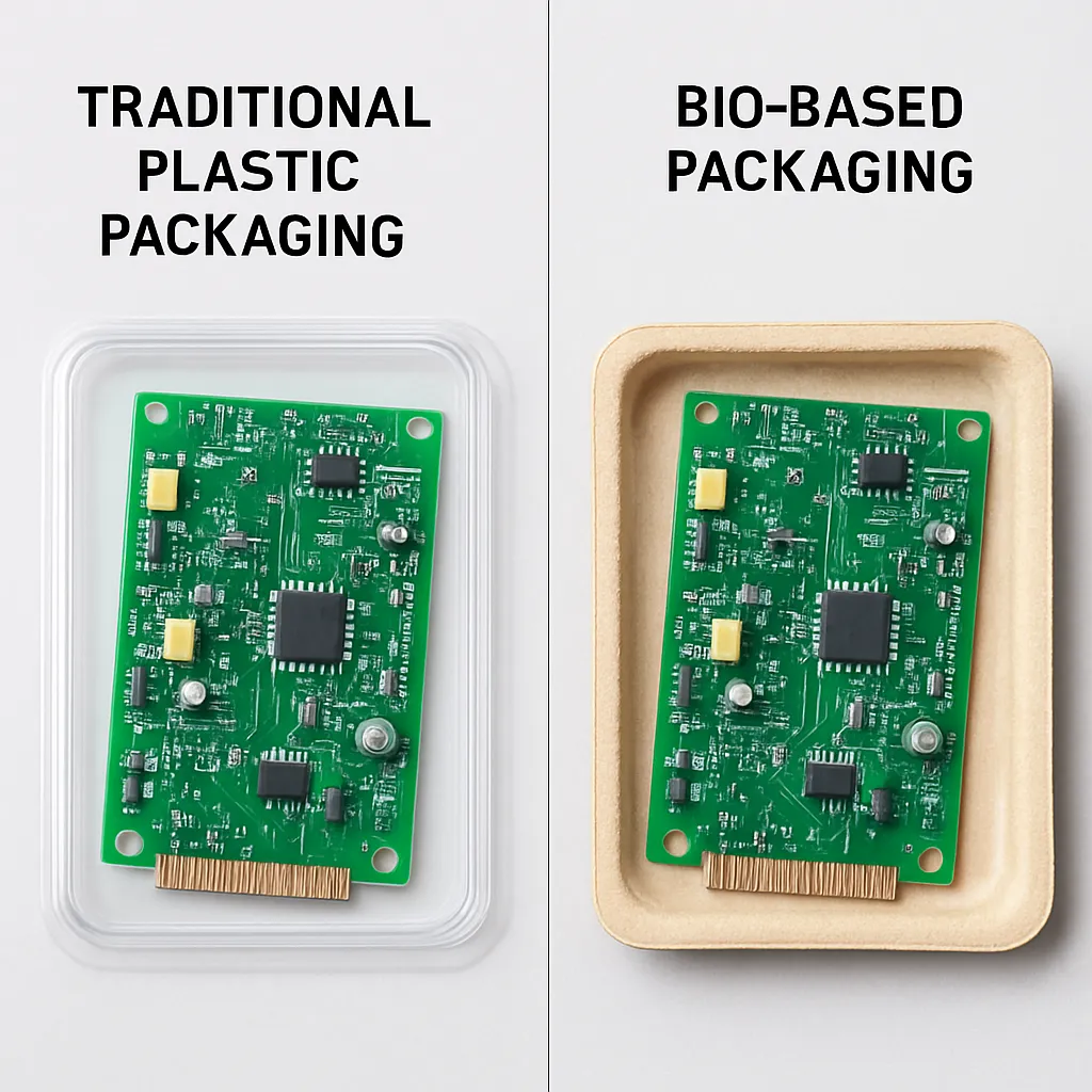
In the fast-evolving world of electronics, protecting printed circuit board (PCB) components during shipping and storage is critical. Traditional packaging materials like plastic and foam often harm the environment, leading to a growing demand for sustainable alternatives. So, how can bio-based solutions like mushroom packaging help? Mushroom packaging, made from mycelium (the root structure of mushrooms), offers a compostable, eco-friendly way to safeguard PCB components while reducing waste. In this blog, we dive deep into mushroom packaging for PCB, explore mycelium packaging for electronics, and highlight other bio-based component packaging innovations that are shaping the future of the industry.
Why Sustainable Packaging Matters for PCB Protection
The electronics industry produces millions of PCBs every year, and each one needs secure packaging to prevent damage from static, moisture, or physical impact. Traditional materials like polystyrene foam and plastic wraps are effective but come with a downside: they take centuries to decompose and contribute to pollution. With environmental regulations tightening and consumers demanding greener solutions, manufacturers are turning to bio-based options.
Sustainable packaging isn’t just about reducing waste—it’s also about maintaining the integrity of sensitive components. For instance, PCBs often require protection against electrostatic discharge (ESD), which can damage circuits with voltages as low as 100 volts. Bio-based materials are now being engineered to meet these technical needs while offering environmental benefits. Let’s explore how mushroom packaging and other bio-based solutions are stepping up to the challenge.
What Is Mushroom Packaging and How Does It Work for PCBs?
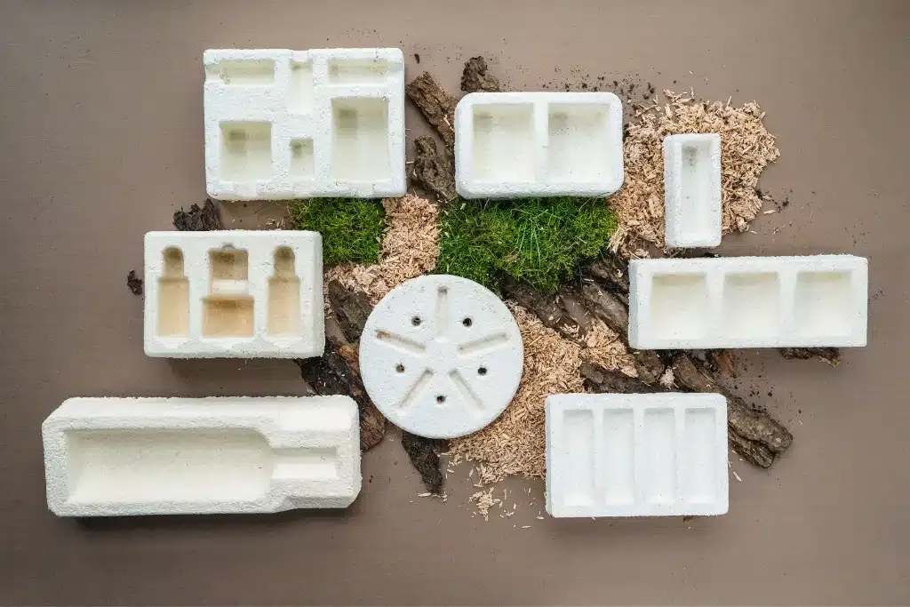
Mushroom packaging is a revolutionary material made from mycelium, the thread-like structure of fungi, combined with agricultural byproducts like hemp or corn stalks. This mixture is grown into specific shapes over a few days, creating a lightweight, durable, and fully compostable material. Companies in the sustainability space have pioneered this technology, showing that it can replace harmful plastics in various industries, including electronics.
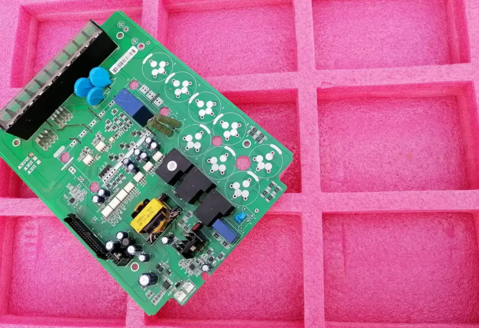
For mushroom packaging in PCB applications, the material can be molded into custom trays or inserts that hold components securely. Its natural shock-absorbing properties help protect delicate circuits from physical damage during transit. Additionally, mycelium-based materials have shown potential for customization—research indicates they can be treated to resist moisture, a critical factor since excessive humidity can corrode PCB traces and reduce signal integrity (often measured at speeds up to 10 Gbps in high-speed designs).
One key advantage is its environmental footprint. Unlike traditional foam, which releases toxic chemicals when incinerated, mushroom packaging breaks down in home compost within 45 days, leaving no harmful residue. This makes it a game-changer for companies looking to lower their carbon footprint while ensuring safe delivery of electronics.
Benefits of Mushroom Packaging for Electronics
- Eco-Friendly: Fully biodegradable and made from renewable resources.
- Customizable: Can be grown into precise shapes for specific PCB layouts.
- Cost-Competitive: Recent data suggests production costs are becoming comparable to single-use plastics, with some estimates showing a price difference of less than 10% as of 2025.
- Shock Absorption: Naturally cushions components against drops or vibrations.
Challenges of Using Mycelium Packaging in Electronics
While mycelium packaging for electronics holds immense promise, it’s not without hurdles. One major concern is its ability to handle extreme conditions. PCBs often face temperature swings during shipping, and mycelium materials may degrade or lose strength above 50°C (122°F) or in high-humidity environments without additional treatment. Researchers are actively working on coatings and additives to improve durability, but widespread adoption in harsh conditions is still in progress.
Another challenge is ESD protection. Standard mushroom packaging lacks the conductive or dissipative properties needed to prevent static buildup, which can ruin sensitive components like microcontrollers or capacitors. However, innovations are emerging—some bio-based materials are now being infused with natural conductive elements to address this issue, though they’re not yet as effective as synthetic ESD-safe foams that meet standards like ANSI/ESD S20.20.
Despite these challenges, the potential for mycelium packaging remains high. As R&D continues, we can expect solutions that balance sustainability with the strict technical demands of electronics protection.
Beyond Mushroom Packaging: Other Bio-Based Component Packaging Solutions
While mushroom packaging is a frontrunner, other bio-based component packaging options are gaining traction in the electronics industry. These alternatives also aim to replace non-degradable materials with sustainable ones, ensuring PCB components are protected without harming the planet.
1. Bioplastics for PCB Protection
Bioplastics, derived from renewable sources like corn starch or sugarcane, are being used to create protective films and enclosures for electronics. Unlike traditional plastics, bioplastics can decompose under industrial composting conditions. Some bioplastic films offer tensile strength comparable to polyethylene, with breaking points around 20-30 MPa, making them suitable for wrapping PCBs during shipping.
However, bioplastics often require specific conditions to break down, which may not be available everywhere. Their production can also be energy-intensive, offsetting some environmental benefits. Still, they represent a viable step toward greener packaging.
2. Cellulose-Based Materials
Cellulose, sourced from wood pulp or recycled paper, is another promising material for PCB packaging. It can be formed into rigid trays or soft padding, offering moderate shock resistance. Recent advancements have led to cellulose composites with improved moisture barriers, critical for preventing corrosion on PCB solder joints exposed to humidity levels above 60%.
Cellulose materials are widely recyclable and often cheaper than mycelium-based options, making them a practical choice for large-scale production. Their main limitation is lower durability compared to plastics or mushroom packaging, especially for heavy or complex PCB assemblies.
3. Agricultural Waste Composites
Packaging made from agricultural waste, such as rice husks or wheat straw, combined with natural binders, is another innovative solution. These composites can be molded into protective casings for electronics, providing decent impact resistance. Some studies show these materials can absorb impacts up to 50% as effectively as expanded polystyrene (EPS) foam in controlled tests.
This approach not only reduces waste but also repurposes materials that would otherwise be discarded. However, consistency in quality and scalability remain challenges for widespread use in the electronics sector.
How Bio-Based Packaging Aligns with Industry Trends in 2025
As of 2025, sustainability is no longer just a buzzword—it’s a core driver of innovation in the electronics industry. According to recent market insights, the demand for biodegradable packaging solutions is growing at a compound annual growth rate (CAGR) of over 9%, fueled by stricter environmental regulations and consumer awareness. For PCB manufacturers, adopting bio-based component packaging isn’t just about compliance; it’s about staying competitive in a market that values green practices.
Moreover, bio-based materials are becoming more accessible. Production techniques for mycelium and other natural composites have improved, reducing costs and lead times. For example, growing a batch of mushroom packaging now takes as little as 7 days, compared to weeks in earlier iterations. This scalability makes it easier for small and medium-sized enterprises to integrate sustainable solutions without sacrificing profitability.
At the same time, the push for circular economies—where materials are reused or composted rather than discarded—is encouraging collaboration between packaging innovators and electronics manufacturers. This synergy is crucial for developing materials that meet both environmental and technical standards, such as protecting high-speed PCBs with signal integrity requirements up to 25 Gbps.
Practical Steps to Implement Bio-Based Packaging for PCB Protection
Transitioning to sustainable packaging for PCB components doesn’t have to be overwhelming. Here are actionable steps to get started:
- Assess Your Needs: Evaluate the specific requirements of your PCBs, such as size, weight, and sensitivity to static or moisture. This helps determine which bio-based material is the best fit.
- Partner with Innovators: Work with suppliers specializing in mycelium or other bio-based packaging to create custom solutions tailored to your products.
- Test Performance: Conduct rigorous testing to ensure the packaging meets industry standards for shock resistance, ESD protection, and environmental durability. Use metrics like drop test results (e.g., surviving a 1-meter fall) to validate effectiveness.
- Educate Your Team: Train staff on handling and disposing of bio-based materials, especially since some require specific composting conditions.
- Communicate Benefits: Highlight your commitment to sustainability in marketing materials, as eco-conscious practices can attract environmentally aware customers.
The Future of Bio-Based Packaging in Electronics
The journey toward fully sustainable packaging for electronics is just beginning. Innovations in mushroom packaging for PCB and other bio-based materials are paving the way for a greener industry. Researchers are exploring ways to enhance mycelium with natural flame retardants and conductive properties, potentially making it a one-stop solution for all PCB protection needs. Meanwhile, advances in bioplastics and composites promise even more options for manufacturers.
In the next decade, we can expect bio-based packaging to become the norm rather than the exception. As production scales up and costs continue to drop, even the most complex electronics—think multi-layer PCBs with impedance values as tight as 50 ohms—will be shipped in materials that are as kind to the planet as they are effective at protection.
Conclusion: Embracing Sustainability in PCB Packaging
The shift to bio-based solutions like mycelium packaging for electronics marks a turning point for the industry. From mushroom packaging to cellulose trays and agricultural waste composites, these materials offer practical, eco-friendly ways to protect PCB components without compromising on performance. While challenges like ESD protection and durability in extreme conditions remain, ongoing innovations are closing the gap rapidly.
For electronics manufacturers, adopting bio-based component packaging is an opportunity to lead in sustainability while meeting the technical demands of modern circuits. By taking small, strategic steps today, companies can build a future where protecting PCBs and protecting the environment go hand in hand.


