 ALLPCB


In the world of printed circuit board (PCB) manufacturing, ensuring the quality and reliability of every board is critical. One of the most effective ways to achieve this is by maximizing test coverage with flying probe testing. But what exactly does this mean, and how can you optimize it? Flying probe testing coverage refers to the extent to which a PCB's components and connections are tested for electrical performance and defects using automated, movable probes. By focusing on test coverage optimization, manufacturers can detect issues early, reduce costs, and improve product reliability. In this detailed guide, we’ll explore flying probe testing analysis, best practices, and strategies to ensure comprehensive testing for your PCB projects.
What Is Flying Probe Testing and Why Does Coverage Matter?
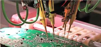
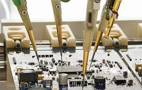
Flying probe testing (FPT) is an automated testing method used in PCB manufacturing to check the electrical integrity of a board. Unlike traditional in-circuit testing (ICT) that requires custom fixtures, FPT uses movable probes that dynamically contact test points on the PCB to identify issues like shorts, opens, and incorrect component values. This flexibility makes it ideal for prototypes, low-volume production, and complex boards with limited test access points.
Test coverage in flying probe testing refers to the percentage of a PCB’s components, nets, and connections that are verified during the testing process. Higher coverage means fewer undetected defects, leading to better quality control. For instance, achieving 95% test coverage on a board with 500 nets means that 475 of those connections have been checked for issues. Missing even 5% can lead to costly failures in the field, making test coverage optimization a priority for manufacturers.
The Importance of Flying Probe Testing Coverage in PCB Manufacturing
In PCB production, defects such as open circuits, short circuits, or incorrect resistor values (e.g., a 1kΩ resistor reading as 1.2kΩ due to manufacturing variance) can cause system failures. Flying probe testing coverage directly impacts the ability to catch these issues before a board reaches assembly or end-use. Comprehensive coverage ensures that even hard-to-reach areas of a high-density PCB are tested, reducing the risk of failures in critical applications like medical devices or automotive electronics.
Moreover, optimizing test coverage with flying probe testing saves time and money. Detecting a short circuit during testing, for example, prevents the need for expensive rework or recalls after a product is shipped. Studies suggest that fixing a defect during the design or testing phase can cost up to 10 times less than addressing it after production.
How Flying Probe Testing Works: A Step-by-Step Overview
Understanding how flying probe testing operates is key to maximizing its coverage. Here’s a breakdown of the process:
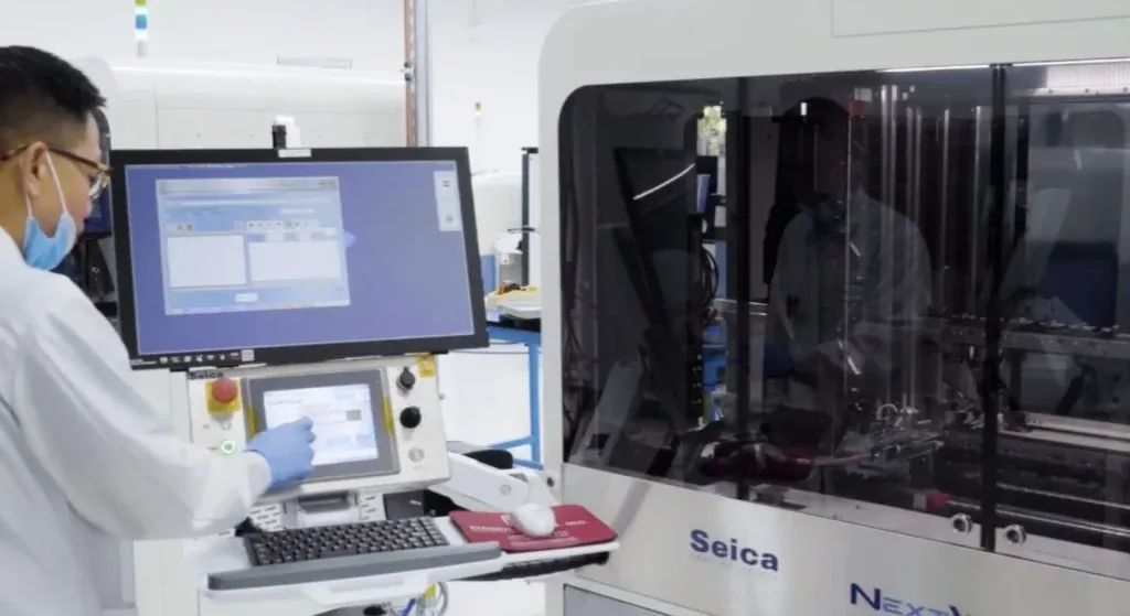
- Programming the Test: Engineers create a test program based on the PCB’s design files, identifying test points for components and nets. This program instructs the probes where to go and what to measure.
- Probe Movement: The machine uses multiple probes (typically 2 to 6) that move independently across the board to contact test points. These probes can measure resistance, capacitance, and continuity at high speeds.
- Data Collection: As probes make contact, the system records electrical values. For example, a probe might measure a capacitor’s value to ensure it matches the specified 10μF rating within a ±5% tolerance.
- Analysis and Reporting: The system compares measured data against expected values, flagging any discrepancies as defects for further investigation.
This process highlights why test coverage optimization is essential—without thorough programming and strategic test point selection, critical areas of the PCB might be missed.
Challenges in Achieving High Flying Probe Testing Coverage
While flying probe testing is highly effective, achieving maximum coverage comes with challenges:
- Limited Test Access: High-density boards with small components or buried vias may have test points that are difficult for probes to reach, reducing coverage.
- Time Constraints: Testing every single net and component increases test duration. For a board with 1,000 test points, full coverage might take several minutes per board, impacting production speed.
- Complex Designs: Modern PCBs often include fine-pitch components or multi-layer designs, complicating test point access and programming.
Overcoming these challenges requires a strategic approach to test coverage optimization, which we’ll explore next.
Test Coverage Optimization Techniques for Flying Probe Testing
To maximize flying probe testing coverage, manufacturers must adopt best practices and innovative strategies. Below are proven techniques to enhance your testing process:
1. Strategic Test Point Selection
Choosing the right test points is the foundation of high coverage. Focus on critical nets and components that are most likely to fail, such as power lines or high-speed signal paths. For example, prioritize testing a net carrying a 3.3V power supply over a less critical ground connection. Use design-for-test (DFT) principles during the PCB layout phase to ensure test points are accessible, ideally spaced at least 2mm apart for probe accuracy.
2. Advanced Programming for Efficiency
Optimize test programs to reduce probe movement and testing time while maintaining coverage. Group test points by proximity so probes travel shorter distances, cutting test time by up to 20%. Additionally, use software tools to simulate test coverage before running the actual test, identifying untested areas for program adjustments.
3. Leveraging Multiple Probes
Modern flying probe testers often support multiple probes working simultaneously. A 4-probe system can test two nets at once, effectively doubling testing speed without sacrificing coverage. Ensure your equipment is configured to handle parallel testing for complex boards with thousands of test points.
4. Combining Flying Probe with Other Methods
For areas where flying probe coverage is limited, such as under BGA (Ball Grid Array) components, complement FPT with other testing methods like boundary scan or X-ray inspection. This hybrid approach can push overall test coverage closer to 100%, ensuring no defect goes undetected.
5. Regular Equipment Calibration
Probe accuracy is vital for reliable measurements. A misaligned probe might fail to contact a test point, falsely reporting an open circuit. Calibrate your flying probe tester regularly to maintain precision, especially when testing components with tight tolerances, like a 0.1% precision resistor.
Flying Probe Testing Analysis: Measuring and Improving Coverage
Flying probe testing analysis involves evaluating the effectiveness of your test process and identifying gaps in coverage. Start by generating a coverage report after each test run. Most modern testers provide software that details which nets and components were tested and which were missed. For instance, a report might show that 92% of nets were tested, with 8% inaccessible due to design constraints.
Use this data to refine your approach. If coverage is below 90%, revisit your test program to add more test points or adjust probe paths. Additionally, track defect escape rates—defects found after testing—to measure real-world effectiveness. If a board passes FPT but fails in functional testing due to an untested net, it’s a sign that coverage needs improvement.
Flying Probe Testing Best Practices for Maximum Results
Implementing flying probe testing best practices ensures consistent, high-quality results. Here are actionable tips to follow:
- Integrate DFT Early: Work with designers to include testability features like exposed test pads during the PCB layout phase. This can boost coverage by up to 15% on dense boards.
- Update Test Programs: As PCB designs evolve, so should test programs. Regularly update them to account for design changes or new components.
- Focus on High-Risk Areas: Prioritize testing areas prone to failure, such as high-speed signal lines with impedance requirements (e.g., 50Ω for USB signals).
- Train Your Team: Ensure operators and engineers are well-versed in flying probe technology to minimize programming errors and maximize coverage.
- Monitor Test Times: Balance coverage with efficiency. If testing a board takes over 5 minutes due to exhaustive checks, consider partial coverage for non-critical areas to speed up production.
Benefits of Optimized Flying Probe Testing Coverage
Investing in test coverage optimization through flying probe testing yields significant benefits:
- Improved Product Quality: Higher coverage means fewer undetected defects, resulting in more reliable PCBs for end users.
- Cost Savings: Catching defects early reduces rework costs. For example, fixing a short during testing might cost $1 per board, compared to $10 or more after assembly.
- Faster Time-to-Market: Efficient testing processes, even with high coverage, streamline production and prevent delays caused by quality issues.
- Flexibility for Prototypes: Flying probe testing’s fixtureless nature makes it perfect for small runs or design iterations, where full coverage ensures prototypes are ready for validation.
Conclusion: Elevate Your PCB Testing with Flying Probe Strategies
Maximizing test coverage with flying probe testing is a game-changer for PCB manufacturing. By focusing on flying probe testing coverage, employing test coverage optimization techniques, conducting thorough flying probe testing analysis, and following flying probe testing best practices, manufacturers can ensure their boards meet the highest quality standards. Whether you’re producing prototypes or scaling up for mass production, a comprehensive approach to FPT helps catch defects early, save costs, and build trust with your customers.
Start by evaluating your current test coverage and implementing the strategies outlined in this guide. With the right tools, programming, and focus on continuous improvement, you can achieve near-perfect coverage and deliver flawless PCBs every time.


