 ALLPCB


If you're an electronics engineer looking to perfect the art of PCB manufacturing, understanding the PCB plasma etching process is crucial. This advanced technique ensures precision in creating intricate circuit patterns by removing unwanted material with high accuracy. In this guide, we'll dive deep into plasma etching, covering essential topics like plasma etching parameters, RF plasma etching, ICP plasma etching, and plasma etching equipment. Whether you're new to the field or seeking to refine your skills, this blog will provide actionable insights to elevate your PCB production process.
What is PCB Plasma Etching and Why Does It Matter?
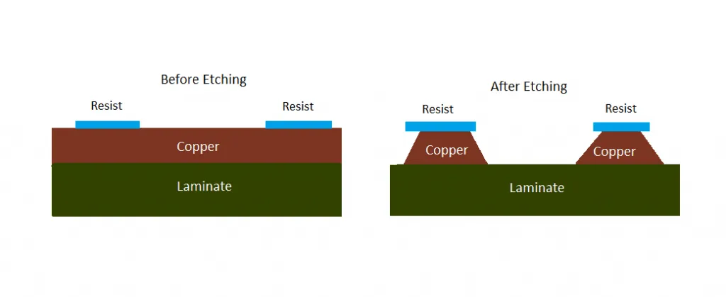
Plasma etching is a dry etching technique used in PCB manufacturing to remove material from a substrate using a high-energy plasma of reactive gases. Unlike traditional wet etching, which uses chemical solutions, plasma etching offers superior precision and control, making it ideal for creating fine patterns on printed circuit boards (PCBs). This process is widely used in the semiconductor industry and advanced electronics manufacturing to achieve high-resolution features, often down to the nanometer scale.
For electronics engineers, mastering plasma etching means producing PCBs with tighter tolerances and better performance. It’s a critical step in fabricating modern devices where miniaturization and accuracy are non-negotiable. Let’s explore the fundamentals of this process and how it can benefit your projects.
Understanding the PCB Plasma Etching Process
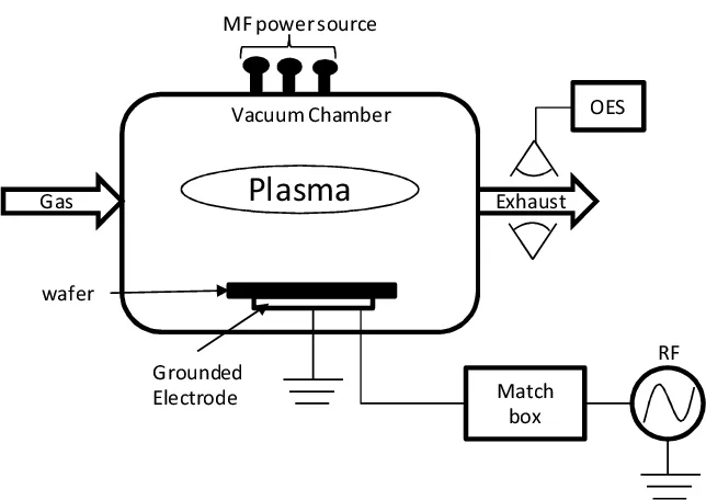
The PCB plasma etching process involves using a plasma—a partially ionized gas containing positive ions, electrons, and neutral atoms—to etch away specific areas of a substrate. Here’s a step-by-step breakdown of how it works:
- Setup and Preparation: The PCB substrate, often coated with a photoresist mask, is placed in a vacuum chamber. The mask defines the areas to be etched and those to be protected.
- Gas Introduction: Reactive gases, such as fluorine or chlorine-based compounds, are introduced into the chamber. The choice of gas depends on the material being etched, like copper or dielectric layers.
- Plasma Generation: An electric field, typically created by radio frequency (RF) power, ionizes the gas, forming plasma. This plasma contains highly reactive species that interact with the exposed substrate material.
- Etching: The reactive species chemically react with the substrate, forming volatile byproducts that are removed from the chamber. Simultaneously, ions in the plasma can physically bombard the surface, enhancing the etching rate through a process called sputtering.
- Completion: Once the desired depth or pattern is achieved, the process stops, and the PCB is cleaned to remove any residual mask or byproducts.
This process allows for anisotropic etching, meaning it can create vertical sidewalls with minimal undercutting, which is essential for high-density PCB designs. For instance, achieving feature sizes as small as 100 nanometers is possible with optimized plasma etching setups, a feat unattainable with wet etching methods.
Key Plasma Etching Parameters for Optimal Results
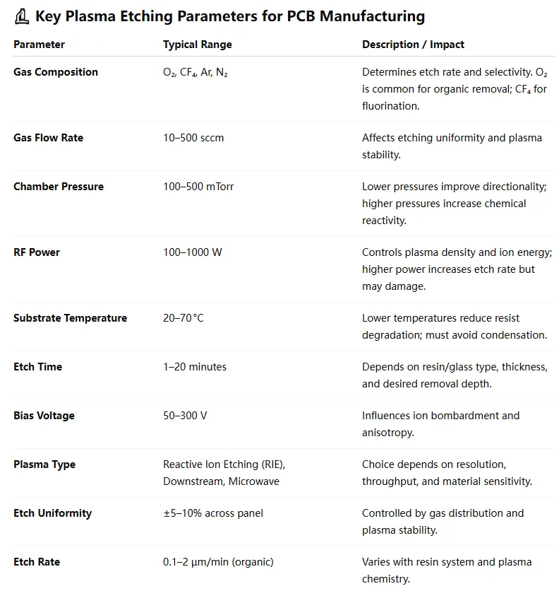
To achieve the best outcomes in plasma etching, engineers must carefully control several parameters. Adjusting these settings can significantly impact etch rate, uniformity, and selectivity (the ability to etch one material over another). Here are the critical plasma etching parameters to monitor:
- RF Power: The power level, often ranging from 100 to 1000 watts, determines the energy of the plasma. Higher power increases the etch rate but can also lead to more physical sputtering, potentially damaging delicate features.
- Pressure: Chamber pressure, typically between 1 to 100 millitorr, affects plasma density and ion energy. Lower pressures result in more directional etching, ideal for anisotropic profiles.
- Gas Flow Rate: The rate at which reactive gases are introduced, measured in standard cubic centimeters per minute (sccm), influences the concentration of reactive species. For example, a flow rate of 20-50 sccm is common for fluorine-based etching of silicon.
- Gas Composition: The mix of gases determines the chemical reactions during etching. Adding oxygen to a fluorine-based plasma can enhance the etching of organic materials on a PCB.
- Substrate Temperature: Keeping the substrate at a controlled temperature, often between 20°C to 80°C, helps manage etch uniformity and prevents thermal damage.
Fine-tuning these parameters requires experimentation and monitoring. For instance, increasing RF power from 200 to 500 watts might boost the etch rate by 30%, but it could also reduce selectivity, etching unintended materials. Engineers must balance speed with precision to meet design specifications.
Exploring RF Plasma Etching: The Backbone of Modern Etching
RF plasma etching, or radio frequency plasma etching, is one of the most common methods used in PCB manufacturing. It relies on a 13.56 MHz RF power source to generate plasma in a capacitively coupled system. This technique is valued for its simplicity and versatility in etching various materials, from metals to insulators.
In an RF plasma etching setup, two electrodes create an electric field that ionizes the gas. The substrate is placed on one electrode, often the powered one, where it experiences both chemical reactions and ion bombardment. This dual mechanism allows RF plasma etching to achieve moderate etch rates, typically around 50-200 nanometers per minute for copper layers, depending on the gas mix and power settings.
One advantage of RF plasma etching is its compatibility with a wide range of equipment and materials. However, it may struggle with high-density plasma requirements for ultra-fine features, where other methods like ICP plasma etching excel.
ICP Plasma Etching: Taking Precision to the Next Level
Inductively Coupled Plasma (ICP) etching is an advanced form of plasma etching that offers higher plasma density and better control over ion energy. Unlike RF plasma etching, which uses capacitive coupling, ICP employs an inductive coil to generate plasma, resulting in densities up to 10^12 electrons per cubic centimeter—significantly higher than traditional RF systems.
ICP plasma etching is particularly useful for creating deep, narrow features on PCBs, such as trenches or vias with aspect ratios exceeding 10:1. Its ability to separate ion energy from plasma density allows engineers to fine-tune the process for anisotropic etching without excessive physical damage. For example, ICP systems can achieve etch rates of 300-500 nanometers per minute for dielectric materials while maintaining sidewall angles close to 90 degrees.
This method is ideal for advanced PCB designs requiring sub-micron precision. However, ICP equipment is more complex and costly, making it a choice for high-end applications rather than standard PCB production.
Choosing the Right Plasma Etching Equipment
Selecting the appropriate plasma etching equipment is a critical decision for electronics engineers. The choice depends on factors like production volume, feature size, and budget. Here are key considerations when evaluating plasma etching systems:
- Type of System: Decide between RF and ICP systems based on your precision needs. RF systems are more affordable and suitable for general-purpose etching, while ICP systems cater to high-density, high-precision tasks.
- Chamber Size: Ensure the equipment can accommodate your PCB dimensions. Industrial systems often support substrates up to 300 mm in diameter, while smaller setups handle 100-150 mm boards.
- Power Range: Look for equipment with adjustable RF power, ideally from 100 to 2000 watts, to cover a variety of etching scenarios.
- Gas Handling: The system should support multiple gas inputs with precise flow control for flexibility in etching different materials.
- Automation and Monitoring: Advanced systems with real-time monitoring of parameters like pressure and etch depth improve consistency and reduce errors.
Investing in reliable plasma etching equipment can significantly enhance your manufacturing capabilities. For small-scale or prototype work, a compact RF system might suffice, while mass production of complex PCBs may justify the cost of an ICP system.
Best Practices for Effective Plasma Etching in PCB Manufacturing
To maximize the benefits of plasma etching, follow these best practices tailored for electronics engineers:
- Optimize Mask Design: Use high-quality photoresist or hard masks to ensure precise pattern transfer. Poor mask integrity can lead to uneven etching or defects.
- Monitor Etch Uniformity: Regularly check etch depth and sidewall profiles across the PCB to detect variations early. Uniformity issues often stem from uneven plasma distribution.
- Control Contamination: Maintain a clean chamber environment to prevent particles from interfering with the etching process. Routine maintenance, such as chamber cleaning after every 10-15 runs, is essential.
- Test Small Batches: Before full-scale production, run test batches to fine-tune parameters. Adjust RF power or gas flow incrementally to avoid over-etching.
- Document Results: Keep detailed records of parameter settings and outcomes for each etching run. This data helps in troubleshooting and replicating successful processes.
By adhering to these practices, you can achieve consistent, high-quality results in your PCB plasma etching projects.
Common Challenges in Plasma Etching and How to Overcome Them
Even with the best equipment and practices, plasma etching can present challenges. Here are some common issues and solutions:
- Non-Uniform Etching: Caused by uneven plasma distribution or substrate placement. Ensure the PCB is centered in the chamber and consider using a rotating stage for better uniformity.
- Over-Etching: Occurs when etching continues beyond the target depth, damaging underlying layers. Use endpoint detection systems to stop the process at the right moment.
- Low Selectivity: When the plasma etches unintended materials, adjust the gas composition or reduce RF power to enhance chemical specificity over physical sputtering.
- Residue Formation: Leftover material or byproducts can contaminate the PCB. Incorporate a post-etch cleaning step using oxygen plasma to remove organic residues.
Addressing these challenges requires patience and iterative adjustments, but the results—clean, precise PCB patterns—are well worth the effort.
Conclusion: Elevate Your PCB Manufacturing with Plasma Etching
Mastering the PCB plasma etching process is a game-changer for electronics engineers. By understanding key aspects like plasma etching parameters, the differences between RF and ICP plasma etching, and the right equipment choices, you can achieve unparalleled precision in your PCB designs. This comprehensive guide has walked you through the essentials, from the basic process to advanced troubleshooting tips, ensuring you have the knowledge to tackle any etching project with confidence.
Whether you're working on prototypes or high-volume production, plasma etching offers the control and accuracy needed for modern electronics. Start by experimenting with the parameters and practices outlined here, and watch as your PCB manufacturing reaches new heights of quality and efficiency.


