 ALLPCB


In today’s fast-paced, technology-driven world, the Internet of Things (IoT) is transforming how we live and work. From smart thermostats to wearable fitness trackers, connected devices are everywhere, and their demand is skyrocketing. But what powers these innovative gadgets behind the scenes? The answer lies in carefully designed and mass-produced printed circuit boards (PCBs). This blog dives deep into the critical role of PCB design for IoT devices and the challenges and solutions in mass production of PCBs for IoT. We’ll explore key aspects like wireless PCB design, antenna design for PCBs, and low power PCB design to help engineers and manufacturers meet the unique demands of connected devices.
Why PCBs Are the Backbone of IoT Devices
IoT devices are all about connectivity, efficiency, and compactness. Whether it’s a smartwatch sending data to your phone or a sensor monitoring industrial equipment, every IoT device relies on a PCB to house its electronic components and ensure seamless operation. PCBs act as the foundation, connecting microcontrollers, sensors, wireless modules, and power systems in a tiny, efficient package.
The challenge, however, is that IoT applications have unique requirements compared to traditional electronics. These devices often need to be small, consume minimal power, and support wireless communication—all while being produced at scale to meet market demands. This is where specialized PCB design for IoT devices and strategic mass production of PCBs for IoT come into play.
Key Challenges in PCB Design for IoT Devices
Designing PCBs for IoT devices isn’t a straightforward task. Engineers face several hurdles to ensure functionality, reliability, and cost-effectiveness. Let’s break down some of the major challenges.
1. Miniaturization and Space Constraints
IoT devices are often tiny, requiring PCBs to fit into extremely limited spaces. Think of a fitness tracker or a smart sensor—there’s no room for bulky boards. This means engineers must use high-density interconnect (HDI) technology and multi-layer designs to pack more components into smaller areas. For instance, a typical IoT PCB might use traces as narrow as 0.1 mm to maximize space efficiency.
2. Power Efficiency
Many IoT devices run on batteries, so low power PCB design is critical. A poorly designed board can drain a battery in hours, making the device impractical. Engineers often incorporate power-saving components like low-power microcontrollers and optimize circuit layouts to minimize energy loss. For example, reducing parasitic capacitance in the design can cut power consumption by up to 15% in some cases.
3. Wireless Connectivity
Wireless PCB design is at the heart of IoT, as most devices rely on Wi-Fi, Bluetooth, or cellular networks to communicate. This requires careful placement of components to avoid signal interference and ensure reliable data transmission. A common issue is electromagnetic interference (EMI), which can disrupt signals if traces are not properly routed or grounded.
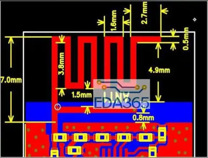
4. Antenna Integration
Antenna design for PCBs is another critical factor in IoT. Many devices use embedded antennas directly on the PCB to save space, but this comes with challenges. The antenna must be tuned to specific frequencies (like 2.4 GHz for Wi-Fi) and positioned away from noisy components to avoid performance issues. A poorly designed antenna can reduce signal range by as much as 30%, impacting the device’s usability.
Solutions for Effective PCB Design for IoT Devices
Overcoming the challenges of IoT PCB design requires a combination of innovative techniques and best practices. Here are some proven solutions to ensure your boards meet the demands of connected devices.
1. Leveraging Advanced Design Tools
Modern design software allows engineers to simulate and test PCB layouts before production. These tools can model signal integrity, thermal performance, and EMI, helping to identify issues early. For instance, simulation can show if a trace layout causes signal delays at high frequencies, allowing for adjustments before manufacturing.
2. Prioritizing Low Power PCB Design
To achieve low power PCB design, engineers can use components like ultra-low-power microcontrollers that consume as little as 1 μA in sleep mode. Additionally, optimizing the board layout to shorten trace lengths reduces resistance and power loss. Techniques like power gating—turning off unused sections of the circuit—can further extend battery life.
3. Optimizing Wireless PCB Design
For wireless PCB design, proper grounding and shielding are essential to minimize EMI. Engineers often use a ground plane beneath sensitive traces to reduce noise. Additionally, keeping high-speed signal traces short and straight prevents signal degradation. For example, maintaining a 50-ohm impedance for RF traces ensures optimal performance in wireless communication.
4. Fine-Tuning Antenna Design for PCBs
Antenna design for PCBs requires precision. Engineers must calculate the antenna’s dimensions based on the target frequency and ensure there’s a clear “keep-out” zone around it to avoid interference. Tools like network analyzers can measure the antenna’s return loss (S11 parameter) to confirm it’s tuned correctly—values below -10 dB are typically ideal for good performance.
Mass Production of PCBs for IoT: Scaling Up Without Sacrificing Quality
Once a PCB design is finalized, the next hurdle is mass production of PCBs for IoT. Producing thousands or millions of boards for connected devices demands efficiency, precision, and cost control. Let’s look at the key considerations and strategies for successful mass production.
1. Design for Manufacturability (DFM)
DFM is the practice of designing PCBs with manufacturing in mind. This means avoiding overly complex layouts that increase production costs or error rates. For example, using standard component sizes and minimizing the number of vias can reduce assembly time and defects. A well-executed DFM approach can cut production costs by up to 20% while maintaining quality.
2. Material Selection for Cost and Performance
Choosing the right materials is crucial in mass production. For IoT PCBs, FR-4 is a common, cost-effective substrate for low-frequency applications. However, high-frequency wireless designs might require materials like Rogers or Teflon, which offer better signal integrity but come at a higher cost. Balancing performance with budget is key—especially when producing at scale.
3. Automated Assembly for Efficiency
Mass production relies heavily on automation to place components quickly and accurately. Surface-mount technology (SMT) is widely used for IoT PCBs, as it allows machines to place tiny components with precision. Automated optical inspection (AOI) systems can also scan boards for defects, catching issues like misaligned components or solder bridges before they reach the market.
4. Testing and Quality Control
Quality assurance is non-negotiable in IoT PCB production. Functional testing ensures each board operates as intended, while in-circuit testing (ICT) checks for shorts, opens, and component values. For wireless designs, RF testing confirms antenna performance and signal strength. Implementing rigorous testing protocols can reduce failure rates to less than 1%, ensuring reliability in the field.
Balancing Cost and Innovation in IoT PCB Production
One of the biggest challenges in mass production of PCBs for IoT is striking a balance between innovation and cost. Cutting-edge features like advanced wireless connectivity or ultra-low power consumption often require expensive components or materials. However, scaling production means keeping costs low to remain competitive.
A practical approach is to prioritize features based on the device’s purpose. For example, a simple IoT sensor for home automation may not need a high-end substrate, while a medical wearable might justify the extra cost for reliability. Additionally, partnering with experienced manufacturing services can streamline production and reduce waste, saving costs without compromising quality.
Future Trends in IoT PCB Design and Production
The IoT landscape is constantly evolving, and PCB design and production must keep pace. Here are a few trends shaping the future of this field.
1. Increased Use of Flexible and Wearable PCBs
As IoT expands into wearables and flexible electronics, PCBs are moving beyond rigid boards. Flexible substrates allow devices to bend and conform to unique shapes, opening new possibilities for design. This trend requires new manufacturing techniques and materials to ensure durability during mass production.
2. Integration of AI and Machine Learning
Artificial intelligence (AI) is making its way into PCB design tools, helping engineers optimize layouts for power and signal integrity. AI can analyze thousands of design variations in minutes, identifying the most efficient configurations for IoT devices. This technology promises to speed up design cycles and improve outcomes in mass production.
3. Growth of 5G and High-Speed Connectivity
The rollout of 5G networks is driving demand for IoT devices with faster, more reliable connectivity. This means wireless PCB design and antenna design for PCBs must evolve to handle higher frequencies (up to 28 GHz or more) and tighter signal tolerances. Manufacturers will need to adopt advanced materials and testing methods to meet these requirements.

Conclusion: Powering the IoT Revolution with PCB Excellence
The rise of IoT is reshaping technology, and PCBs are at the core of this revolution. From tackling the challenges of PCB design for IoT devices to mastering the mass production of PCBs for IoT, engineers and manufacturers must navigate a complex landscape of size, power, and connectivity demands. By focusing on low power PCB design, optimizing wireless PCB design, and perfecting antenna design for PCBs, it’s possible to create reliable, efficient connected devices that meet market needs.
At the same time, strategic approaches to mass production—such as design for manufacturability, automation, and rigorous testing—ensure that quality doesn’t suffer as volumes increase. As IoT continues to grow, staying ahead of trends like flexible PCBs and 5G connectivity will be essential for success. With the right expertise and tools, the possibilities for innovation in IoT PCB design and production are limitless, paving the way for a more connected future.


