 ALLPCB


Designing a printed circuit board (PCB) for high-volume manufacturing can be a complex puzzle. How do you ensure your design is efficient, cost-effective, and ready for mass production? The answer lies in mastering design for manufacturability (DFM) principles tailored for PCBs. By focusing on DFM guidelines for PCB mass production, optimizing PCB layout for production, strategic component placement for high-volume PCB manufacturing, and reducing PCB cost with design tweaks, you can streamline the process and achieve reliable results.
In this comprehensive guide, we’ll break down the essential strategies to optimize your PCB design for high-volume manufacturing. Whether you’re an engineer looking to cut costs or a project manager aiming for seamless production, this post will provide actionable insights to help you succeed. Let’s dive into the world of PCB design optimization and unlock the secrets to efficient mass production.
What Is Design for Manufacturability (DFM) in PCB Design?
Design for Manufacturability (DFM) is a set of practices that ensures a PCB design can be produced efficiently and reliably at scale. When applied to PCB design, DFM focuses on minimizing errors, reducing costs, and speeding up the manufacturing process. For high-volume production, DFM becomes even more critical as small design flaws can lead to significant delays or increased expenses when multiplied across thousands of units.
DFM in PCB design involves everything from choosing the right materials and components to optimizing the layout for automated assembly. By following DFM guidelines for PCB mass production, you can avoid common pitfalls like poor component spacing, unmanufacturable trace widths, or incompatible materials. The goal is simple: design a board that can be built quickly, accurately, and at the lowest possible cost.
Why DFM Matters for High-Volume Manufacturing
In high-volume manufacturing, even a minor design oversight can result in thousands of defective units. For instance, if a trace width is too narrow—say, below 6 mils (0.006 inches)—it might not withstand the current load or could break during fabrication, leading to costly rework. DFM helps identify such issues early in the design phase, saving time and money.
Key DFM Guidelines for PCB Mass Production
To achieve a successful high-volume PCB run, following established DFM guidelines is essential. These rules help ensure that your design aligns with manufacturing capabilities and avoids common production bottlenecks. Below are some critical DFM guidelines tailored for mass production.
1. Standardize Components and Materials
Using standard, widely available components reduces costs and lead times. Avoid exotic or hard-to-source parts unless absolutely necessary. For example, opting for a common resistor value like 1 kΩ instead of a rare 1.03 kΩ can prevent delays in procurement during high-volume runs.
Additionally, stick to standard PCB materials like FR-4 for most designs. While advanced materials like high-frequency laminates may be needed for specific applications, they often come with higher costs and longer lead times, which can slow down mass production.
2. Maintain Proper Clearances and Spacing
Clearance and spacing are critical to prevent issues like short circuits or soldering defects during automated assembly. For high-volume production, adhere to minimum spacing rules, such as maintaining at least 8 mils (0.008 inches) between traces and pads. This ensures that pick-and-place machines and soldering equipment can operate without errors.
3. Optimize for Automated Assembly
Most high-volume PCB production relies on automated assembly lines. Design your board with this in mind by ensuring components are placed on a grid that aligns with pick-and-place machine capabilities. Also, avoid placing components too close to the board edges—maintain at least a 0.1-inch (2.54 mm) margin to prevent damage during handling.
PCB Layout Optimization for Production
A well-optimized PCB layout is the backbone of efficient high-volume manufacturing. PCB layout optimization for production focuses on arranging components and traces in a way that minimizes errors, reduces assembly time, and ensures signal integrity. Here are some proven strategies to achieve this.
1. Minimize Layer Count
Reducing the number of layers in your PCB design can significantly cut costs. For instance, a 2-layer board is far cheaper to produce than a 6-layer board. Unless your design requires additional layers for complex routing or high-speed signals (e.g., above 100 MHz), stick to the fewest layers possible without compromising performance.
2. Simplify Routing Paths
Complex routing with excessive vias or sharp angles can slow down fabrication and increase the risk of signal degradation. Aim for straight, short traces whenever possible. For high-speed designs, maintain controlled impedance—typically 50 ohms for single-ended signals or 100 ohms for differential pairs—to ensure signal integrity.
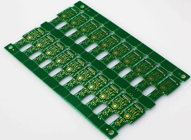
3. Use Panelization for Efficiency
Panelization involves arranging multiple PCB designs on a single manufacturing panel to maximize material usage. For high-volume production, panelization can reduce waste and lower costs. Ensure your design includes proper breakaway tabs or V-scoring to allow easy separation after assembly.
Component Placement for High-Volume PCB Manufacturing
Strategic component placement for high-volume PCB production is crucial for ensuring smooth assembly and minimizing defects. Poor placement can lead to issues like shadowing during soldering or difficulty in automated placement. Here’s how to get it right.
1. Group Similar Components Together
Place components of the same type—such as all resistors or all capacitors—in clusters. This reduces the time pick-and-place machines spend switching between different component reels, speeding up assembly. For example, grouping all 0805-sized resistors in one area can save seconds per board, which adds up in a run of 10,000 units.
2. Orient Components Consistently
Ensure all components, especially polarized ones like diodes and capacitors, are oriented in the same direction. Consistent orientation simplifies programming for automated assembly equipment and reduces the chance of placement errors.
3. Avoid Overcrowding
Overcrowded boards can lead to soldering issues, especially in wave soldering processes used for through-hole components. Maintain at least 0.05 inches (1.27 mm) between components to allow for proper solder flow and to avoid thermal interference during reflow.
Reducing PCB Cost with Design Optimization
Cost is a major concern in high-volume manufacturing. Reducing PCB cost with design optimization doesn’t mean cutting corners—it means making smart choices that lower expenses without sacrificing quality. Here are some effective ways to achieve this.
1. Optimize Board Size
Smaller boards use less material and are cheaper to produce. If possible, reduce the dimensions of your PCB while maintaining functionality. For instance, shrinking a board from 4x4 inches to 3x3 inches can save up to 30% on material costs, depending on the volume.
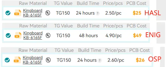
2. Use Cost-Effective Finishes
Surface finishes like HASL (Hot Air Solder Leveling) are more affordable than ENIG (Electroless Nickel Immersion Gold) for most applications. Unless your design requires a premium finish for high-reliability or fine-pitch components, opt for a budget-friendly option.
3. Minimize Custom Features
Custom features like non-standard drill sizes or unique board shapes increase manufacturing complexity and cost. Stick to standard drill sizes (e.g., 0.031 inches or 0.8 mm) and rectangular board shapes to keep expenses down.
Common Pitfalls to Avoid in High-Volume PCB Design
Even with the best intentions, certain design mistakes can derail high-volume production. Being aware of these pitfalls can save you from costly delays. Here are a few to watch out for.
1. Ignoring Manufacturer Capabilities
Not all manufacturers have the same equipment or tolerances. Before finalizing your design, consult with your manufacturing partner to ensure your specifications—such as minimum trace width or drill size—are within their capabilities. For example, some manufacturers may struggle with trace widths below 5 mils (0.005 inches).
2. Overlooking Thermal Management
In high-volume runs, thermal issues can compound quickly if not addressed. Ensure your design includes adequate heat dissipation, such as thermal vias or copper pours, especially for power-heavy components dissipating over 1 watt of heat.
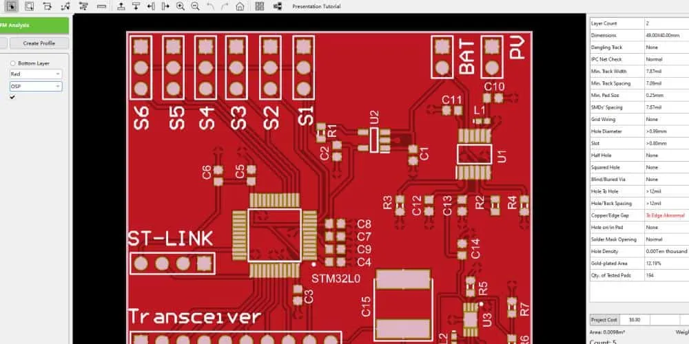
3. Skipping DFM Checks
Always run a DFM analysis before sending your design to production. Many design software tools can flag potential issues like insufficient clearances or unmanufacturable features. Skipping this step can lead to expensive rework after fabrication begins.
Tools and Resources for DFM in PCB Design
Leveraging the right tools can make a big difference in optimizing your PCB for high-volume manufacturing. Many design software platforms offer built-in DFM checks to identify potential issues early. Look for features like automated spacing verification, impedance calculators, and panelization wizards to streamline your process.
Additionally, collaborating with your manufacturing partner during the design phase can provide valuable feedback. They can offer insights into their specific processes and help tailor your design for maximum efficiency.
Conclusion: Mastering PCB Design for High-Volume Success
Optimizing PCB design for high-volume manufacturing is all about planning ahead and making informed decisions. By embracing design for manufacturability (DFM) principles, following DFM guidelines for PCB mass production, focusing on PCB layout optimization for production, ensuring strategic component placement for high-volume PCB runs, and reducing PCB cost with design tweaks, you can achieve efficient and cost-effective results.
Every step, from standardizing components to minimizing layer count, plays a role in cracking the code of high-volume PCB production. With these strategies in hand, you’re well-equipped to create designs that not only meet performance requirements but also excel in the manufacturing environment. Start applying these tips to your next project and watch your production process become smoother and more profitable.


