 ALLPCB


In the world of PCB (Printed Circuit Board) manufacturing, achieving high-quality imaging is crucial for ensuring the functionality and reliability of electronic devices. However, balancing quality with budget constraints is often a challenge for engineers and businesses. If you're searching for affordable PCB imaging solutions or ways to minimize costs without sacrificing precision, you're in the right place. This guide from ALLPCB dives deep into strategies for low-cost PCB inspection, budget-friendly approaches to imaging, and tips for optimizing your spending while maintaining top-tier results.
Whether you're a startup working on a prototype or a large-scale manufacturer, we'll explore practical ways to manage PCB imaging equipment price concerns and reduce overall expenses. Let’s get started with actionable insights to help you strike the perfect balance between cost and quality.
Why PCB Imaging Matters in Manufacturing
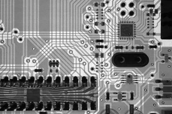
PCB imaging is a critical step in the manufacturing process. It involves transferring the design layout onto the board material, typically through photolithography or direct imaging techniques. This process defines the traces, pads, and vias that form the circuit's structure. Any errors or inconsistencies in imaging can lead to faulty connections, signal interference, or complete board failure.
For engineers, the stakes are high. A single imaging defect can result in costly rework or scrapped boards. This is why investing in reliable imaging solutions is essential. However, high-end equipment and processes often come with steep price tags, making minimizing PCB imaging costs a top priority for many businesses.
Understanding the Cost Factors in PCB Imaging
To find affordable PCB imaging solutions, it’s important to understand what drives the costs. Here are the key factors that influence expenses in PCB imaging:
- Equipment Costs: High-precision imaging machines, such as laser direct imaging (LDI) systems, can cost anywhere from $50,000 to over $200,000 depending on the model and capabilities. These systems offer superior accuracy but may not be feasible for smaller operations.
- Material Costs: The photoresist materials and films used in traditional photolithography can add up, especially for high-volume production. Costs can range from $5 to $20 per square meter of material.
- Labor and Time: Skilled technicians are needed to operate imaging equipment and perform quality checks. Labor costs vary by region but can significantly impact the overall budget.
- Resolution and Complexity: Designs with finer traces (e.g., below 4 mils or 0.1 mm) require more advanced imaging systems, increasing costs due to the need for tighter tolerances and higher resolution.
- Volume: Low-volume runs often have higher per-unit imaging costs compared to mass production, where expenses can be spread across thousands of units.
By understanding these cost drivers, you can make informed decisions to optimize spending while still achieving high-quality results. Let’s explore how to approach budget-friendly PCB manufacturing with imaging in mind.
Strategies for Low-Cost PCB Inspection and Imaging
Finding low-cost PCB inspection and imaging solutions doesn’t mean cutting corners on quality. Here are proven strategies to help you save money while maintaining precision:
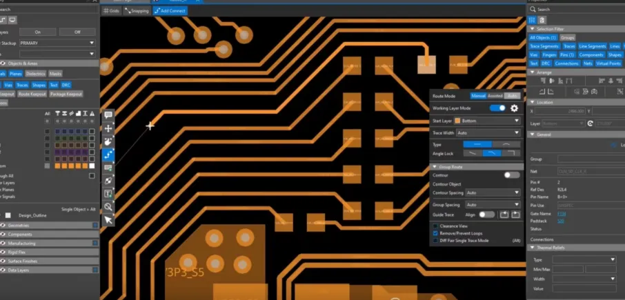
1. Choose the Right Imaging Technology for Your Needs
Not all projects require the most expensive imaging technology. For simpler designs with larger trace widths (e.g., 6 mils or 0.15 mm), traditional photolithography using UV exposure and film masks can be a cost-effective choice. This method is often more affordable, with equipment costs starting at around $10,000 for basic setups.
For complex designs requiring high precision, consider sharing access to advanced equipment like LDI systems through a manufacturing partner. This approach avoids the upfront investment of purchasing costly machinery while still benefiting from cutting-edge technology.
2. Optimize Design for Manufacturability
A well-optimized PCB design can reduce imaging costs significantly. For instance, minimizing the number of layers and avoiding ultra-fine traces (below 3 mils or 0.075 mm) can lower the need for high-end imaging systems. Additionally, ensuring proper spacing between traces—typically at least 5 mils (0.127 mm) for standard processes—can prevent imaging errors and reduce rework expenses.
Work closely with your design team to balance performance requirements with manufacturing constraints. Small adjustments in the layout can lead to substantial savings in imaging costs.
3. Partner with a Cost-Effective Manufacturing Service
Collaborating with a reliable PCB manufacturing service can help manage PCB imaging equipment price concerns. Many providers offer access to advanced imaging tools as part of their service, eliminating the need for in-house equipment. This is especially beneficial for small to medium-sized businesses that can’t justify the capital expenditure on high-end machinery.
Look for providers that offer transparent pricing and flexible options for low-volume or prototype runs. This ensures you only pay for what you need, keeping costs in check.
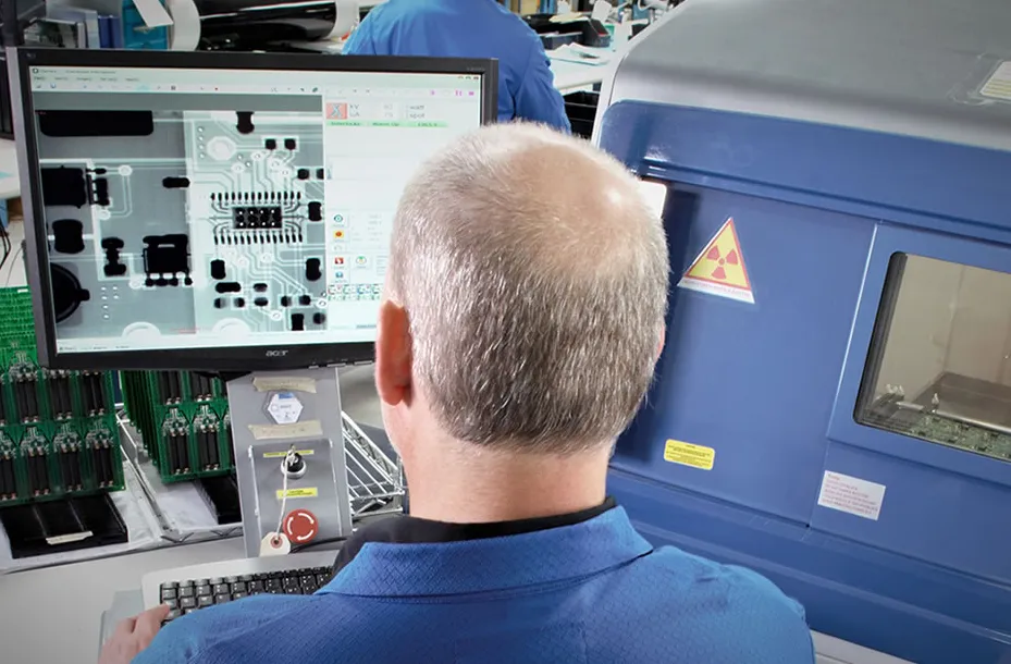
4. Implement Automated Inspection for Cost Savings
Manual inspection of PCBs after imaging can be time-consuming and prone to human error. Automated optical inspection (AOI) systems can streamline low-cost PCB inspection by quickly identifying defects such as misaligned traces or incomplete etching. While AOI equipment can cost between $20,000 and $100,000, the long-term savings from reduced labor and rework often outweigh the initial investment.
For smaller budgets, consider outsourcing inspection to a third-party service that already has AOI capabilities. This can be a more affordable way to ensure quality without the upfront cost.
5. Minimize Waste Through Prototyping
Before committing to a full production run, invest in prototyping to test the imaging process. Identifying issues early—such as incorrect trace impedance (targeting, for example, 50 ohms for high-speed signals)—can prevent costly mistakes during mass production. Prototyping costs are typically low, often under $100 per board for small batches, making it a smart way to save money in the long run.
Balancing Quality and Budget in PCB Imaging
While cost reduction is important, maintaining quality is non-negotiable in PCB manufacturing. Here’s how to ensure you don’t compromise on performance while pursuing budget-friendly PCB manufacturing:
- Prioritize Critical Areas: Focus imaging precision on high-speed or high-frequency sections of the board where signal integrity is crucial. For less critical areas, standard imaging techniques may suffice.
- Regular Calibration: Ensure that imaging equipment is regularly calibrated to avoid errors. Misalignment as small as 1 mil (0.025 mm) can cause signal delays or crosstalk in high-speed designs.
- Quality Materials: Avoid using substandard photoresist or films to save a few dollars. Poor materials can lead to uneven imaging, resulting in defects and costly rework.
- Track Record of Partners: When outsourcing imaging or inspection, choose a manufacturing partner with a proven track record of delivering consistent quality. Check for certifications like ISO 9001 to ensure reliability.
Tools and Technologies for Affordable PCB Imaging
Advancements in technology have made affordable PCB imaging solutions more accessible than ever. Here are some tools and approaches to consider:
- Desktop Imaging Systems: For small-scale operations, desktop UV exposure units are available for under $5,000. These are ideal for prototyping or low-volume production with trace widths above 5 mils (0.127 mm).
- Software Simulation: Use PCB design software with built-in simulation tools to predict imaging outcomes before production. This can help catch potential issues, such as impedance mismatches (e.g., deviations from a 50-ohm target), without wasting materials.
- Cloud-Based Services: Some manufacturing platforms offer cloud-based design and imaging services, allowing you to access professional-grade tools without owning the hardware. This can be a game-changer for startups looking to minimize upfront costs.
Tips for Minimizing PCB Imaging Costs Long-Term
Beyond immediate cost-saving measures, adopting a long-term strategy for minimizing PCB imaging costs can yield even greater benefits. Here’s how to plan ahead:
- Standardize Processes: Develop standardized imaging workflows to reduce variability and errors. Consistency in setup and execution can lower the rate of defects and rework.
- Invest in Training: Equip your team with the skills to operate imaging equipment efficiently. A well-trained staff can prevent costly mistakes and maximize the lifespan of your tools.
- Bulk Purchasing: If you handle materials in-house, buy photoresist and other consumables in bulk to take advantage of volume discounts. Savings of 10-20% per order are common with larger purchases.
- Monitor Trends: Stay updated on emerging imaging technologies that could lower costs in the future. For example, advancements in digital imaging are continuously reducing the PCB imaging equipment price for entry-level systems.
Conclusion: Achieving Cost-Effective PCB Imaging with ALLPCB
Finding the right balance between quality and cost in PCB imaging is entirely possible with the right strategies. By choosing appropriate technologies, optimizing designs, and partnering with experienced manufacturing services, you can achieve budget-friendly PCB manufacturing without compromising on performance. Whether you’re focused on low-cost PCB inspection or exploring affordable PCB imaging solutions, the key lies in making informed decisions tailored to your project’s needs.
Start optimizing your PCB imaging process today by leveraging these tips and partnering with a trusted provider. With the right approach, you can keep costs low while delivering exceptional results for your electronic projects.


