ALLPCB


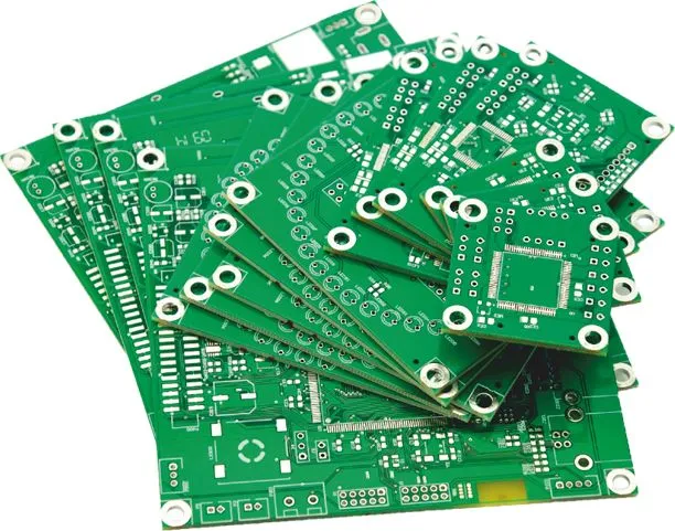
When it comes to creating a PCB prototype, one of the biggest decisions is choosing the right imaging method. Is PCB direct imaging, also known as Laser Direct Imaging (LDI), the best choice for your project, or should you stick with traditional photolithography? For prototypes and low-volume production, the answer often depends on cost, precision, and turnaround time. In short, PCB direct imaging can be a game-changer for prototypes due to its precision and flexibility, saving costs on photomasks and reducing lead times—especially for complex designs or frequent revisions. However, for simpler designs or larger runs, traditional methods might still be more economical.
In this detailed cost-benefit analysis, we'll break down the PCB direct imaging cost, compare direct imaging vs photolithography cost, and explore whether LDI is the right fit for your prototype or low-volume PCB production. Let's dive into the specifics to help you make an informed decision.
What Is PCB Direct Imaging (LDI)?
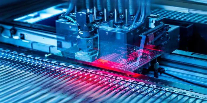
PCB direct imaging, or Laser Direct Imaging (LDI), is a modern technology used in PCB manufacturing to transfer circuit patterns directly onto a photosensitive layer of the board using a laser. Unlike traditional photolithography, which relies on physical photomasks to expose the pattern, LDI uses digital data to control the laser, eliminating the need for masks entirely.
This method offers incredible precision, often achieving resolutions down to 25 micrometers or finer, which is ideal for high-density interconnect (HDI) designs or intricate prototypes. It also speeds up the process since there's no need to create and align masks, making it a popular choice for rapid prototyping.
Understanding Traditional Photolithography
Traditional photolithography has been the standard in PCB manufacturing for decades. It involves creating a photomask—a physical template of the circuit pattern—and using UV light to expose the pattern onto a photosensitive layer on the PCB. While this method is reliable and cost-effective for high-volume production, it has limitations for prototypes and low-volume runs.
For instance, every design change requires a new photomask, which can cost between $500 and $5,000 per mask, depending on complexity. Additionally, the process of aligning masks can introduce errors, especially in finer designs, where even a misalignment of 10 micrometers can cause significant issues.
Cost Breakdown: PCB Direct Imaging vs Photolithography
Let's get into the numbers behind PCB direct imaging cost and compare it with traditional photolithography to understand the financial implications for prototypes and low-volume production.
Initial Equipment and Setup Costs
The upfront investment for LDI is significantly higher than for photolithography. Industrial-grade LDI systems can range from $500,000 to $1,500,000, reflecting the advanced technology and precision they offer. In contrast, a basic photolithography setup might cost between $50,000 and $200,000. For smaller manufacturers or those just starting, this huge difference in equipment cost can be a barrier to adopting LDI.
However, for prototyping services or companies handling multiple projects, the long-term savings with LDI can offset this initial expense. Since LDI doesn't require photomasks, you avoid recurring costs with every new design or revision.
Per-Project Costs for Prototypes
For a single prototype, the PCB prototype cost with LDI can be lower due to the elimination of mask production. A photomask for a complex design might cost $2,000, and if your prototype requires multiple iterations—common in R&D—you could easily spend $6,000 or more just on masks before finalizing the design. With LDI, these costs disappear since the laser directly images the digital design onto the board.
On the other hand, if your prototype design is simple and unlikely to change, the lower setup cost of photolithography might make more sense. For a basic double-layer PCB, a mask might cost only $500, and the overall imaging process could be cheaper than using an LDI system, especially if the equipment cost is factored into service pricing.
Low-Volume Production Costs
For low-volume PCB direct imaging, the cost benefits become even clearer. In batches of 10 to 100 units, the absence of mask costs and the ability to quickly adjust designs without additional expenses make LDI a strong contender. For example, producing 50 units of a complex HDI board with photolithography might incur a mask cost of $3,000 plus additional fees for any design tweaks. With LDI, those costs are avoided, and the per-unit imaging cost remains consistent regardless of design changes.
However, for larger runs of simpler boards (500 units or more), photolithography often regains the advantage. The fixed cost of a photomask becomes negligible when spread across many units, and the faster processing speed of UV exposure can reduce overall production time and cost.
Benefits of PCB Direct Imaging for Prototypes
Beyond the LDI cost analysis, there are several advantages to using direct imaging for prototypes that can influence your decision.
Precision and Quality
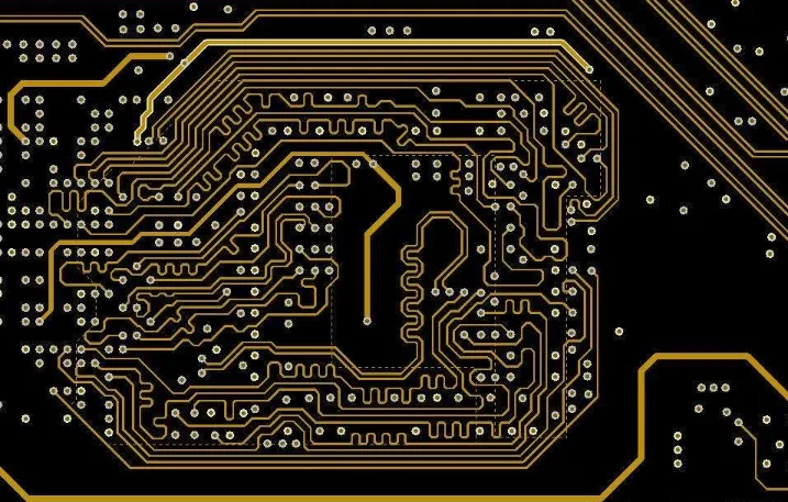
LDI offers unmatched precision, often achieving line widths and spacing as tight as 25 micrometers. This is critical for modern prototypes that include HDI designs or fine-pitch components, where even a small error in imaging can lead to signal integrity issues or board failure. Traditional photolithography, while effective for larger features, struggles with resolutions below 50 micrometers due to mask alignment challenges.
Speed and Flexibility
Prototyping often involves multiple iterations as designs are tested and refined. With LDI, design changes are as simple as updating the digital file—no new masks are needed. This can cut turnaround times from days to hours, a significant advantage when time-to-market is a priority. For example, adjusting a trace width from 6 mils to 5 mils to optimize impedance can be done instantly with LDI, while photolithography would require a new mask and additional lead time.
Reduced Risk of Errors
Since LDI uses digital data directly, there's no risk of mask misalignment or defects in mask production. This reduces the chance of costly rework, especially for prototypes where every error can delay testing and validation.
Drawbacks of PCB Direct Imaging for Prototypes
While LDI has clear advantages, it's not without its challenges, especially when considering the PCB direct imaging cost for smaller operations.
High Initial Investment
As mentioned earlier, the cost of LDI equipment is a significant hurdle. For individual engineers or small startups, accessing LDI might mean partnering with a manufacturer that offers this technology, which could come with higher service fees compared to traditional methods.
Limited Scalability for High Volumes
LDI is slower per board compared to photolithography, as the laser must trace each pattern individually. For prototypes or low-volume runs, this isn't usually an issue, but for larger production, the time cost can outweigh the benefits of mask elimination.
When Should You Choose PCB Direct Imaging?
Deciding between direct imaging and photolithography depends on several factors related to your specific project. Here’s a breakdown to guide your choice:
- Complex Designs: If your prototype involves HDI, fine-pitch components, or tight tolerances (e.g., traces below 3 mils), LDI is likely the better choice for its precision.
- Frequent Iterations: For projects where design changes are expected, such as in early-stage R&D, LDI saves time and money by avoiding repeated mask costs.
- Low-Volume Production: For small batches (under 100 units), low-volume PCB direct imaging is often more cost-effective due to the elimination of upfront mask expenses.
- Budget Constraints: If your project is a simple design with no expected revisions and a tight budget, traditional photolithography might be more economical.
Real-World Example: Prototype Cost Comparison
Let's consider a practical scenario to illustrate the direct imaging vs photolithography cost for a prototype project. Imagine you're developing a 4-layer PCB for a wearable device with fine traces (3 mils) and multiple design iterations expected.
- Photolithography Costs: Initial photomask set for 4 layers costs $4,000. After the first test, you need two design revisions, requiring new masks at $2,000 each, totaling $8,000 in mask costs alone. Add imaging and processing fees of $500, and your total is $8,500 for the prototype phase.
- LDI Costs: With direct imaging, there are no mask costs. The imaging service fee for the same 4-layer board, including revisions, totals $2,500 due to the precision and technology used. Even with a higher per-unit fee, you save $6,000 compared to photolithography.
This example shows how LDI can significantly reduce costs for prototypes with complex designs or iterative processes, despite the higher service fees in some cases.
Tips for Optimizing PCB Prototype Costs
Regardless of the imaging method you choose, there are ways to keep your PCB prototype cost under control:
- Simplify Where Possible: Reduce layer count or relax tolerances if they’re not critical to performance. For example, increasing trace width from 3 mils to 5 mils can lower imaging complexity and cost.
- Plan for Iterations: If using photolithography, finalize as much of the design as possible before ordering masks to avoid costly revisions.
- Partner with Experts: Work with a manufacturing service that offers both LDI and traditional methods, so you can choose the best option based on project needs.
Conclusion: Making the Right Choice for Your Prototype
Choosing between PCB direct imaging and traditional photolithography for your prototype comes down to a careful LDI cost analysis and an understanding of your project's specific needs. Direct imaging shines for complex designs, frequent iterations, and low-volume production, offering precision and flexibility while saving on mask costs. However, for simpler designs or larger runs, the lower upfront cost and faster processing of photolithography might be more practical.
By weighing the PCB direct imaging cost against the benefits of speed, accuracy, and adaptability, you can decide if LDI is the right fit for your next prototype. For engineers and designers looking to balance quality and budget, understanding these trade-offs is the key to efficient and cost-effective PCB development.