 ALLPCB


In the fast-paced world of electronics manufacturing, ensuring the quality of printed circuit boards (PCBs) is critical. While traditional visual inspection has been a staple in quality control, it often falls short in detecting hidden defects or issues in complex, multi-layered boards. So, how can manufacturers guarantee flawless PCBs? Advanced PCB imaging techniques, such as automated optical inspection (AOI), X-ray inspection for PCBs, and other non-destructive PCB testing methods, provide the answer. These cutting-edge technologies enable precise defect detection in PCB imaging, ensuring high-quality outputs for modern electronics.
In this blog, we’ll dive deep into the world of PCB quality control imaging. We’ll explore the limitations of manual inspection and highlight advanced methods that are revolutionizing the industry. Whether you’re an engineer, a manufacturer, or a hobbyist, this guide will help you understand how these technologies work and why they’re essential for producing reliable PCBs.
Why Visual Inspection Isn’t Enough for Modern PCBs
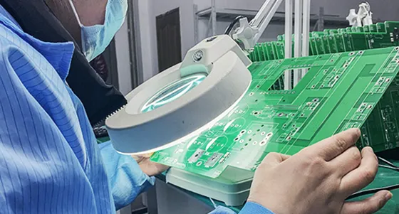
Visual inspection, often done by trained technicians using magnifying tools, has long been a go-to method for spotting surface-level defects on PCBs. Issues like misaligned components, solder bridges, or visible cracks can be caught with the naked eye or basic tools. However, as electronics become smaller and more complex, with components shrinking to sizes as small as 0.4mm x 0.2mm (0402 packages), human inspection struggles to keep up.
Modern PCBs often feature multiple layers—sometimes up to 16 or more—hiding critical connections beneath the surface. Visual checks can’t detect internal defects like voids in solder joints, delamination, or micro-cracks in vias. Missing these issues can lead to failures in the field, costing companies millions in recalls or repairs. According to industry studies, undetected PCB defects account for up to 30% of electronic device failures. This is where advanced PCB quality control imaging steps in, offering non-destructive ways to see beyond the surface.
Automated Optical Inspection (AOI): Precision at High Speed
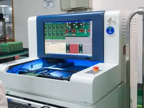
One of the most widely adopted advancements in PCB quality control imaging is Automated Optical Inspection, or AOI. This technology uses high-resolution cameras and sophisticated software algorithms to scan PCBs for surface defects. AOI systems can detect issues like missing components, incorrect placements, solder defects, and even scratches or contamination on the board surface.
Unlike manual inspection, AOI operates at incredible speeds, inspecting hundreds of boards per hour. For instance, a typical AOI system can process a board with over 1,000 components in under 30 seconds. It achieves this by capturing detailed images of the PCB and comparing them to a pre-programmed "golden board" or design file. Any deviation beyond a set tolerance—say, a component misaligned by more than 0.1mm—triggers an alert for further review.
AOI is especially valuable in high-volume production environments where consistency and speed are critical. It reduces human error and cuts down on labor costs while maintaining a high level of accuracy. However, AOI is limited to surface-level inspection and cannot detect issues hidden within the board’s layers. For those, other methods like X-ray inspection come into play.
X-Ray Inspection for PCBs: Seeing Through Layers
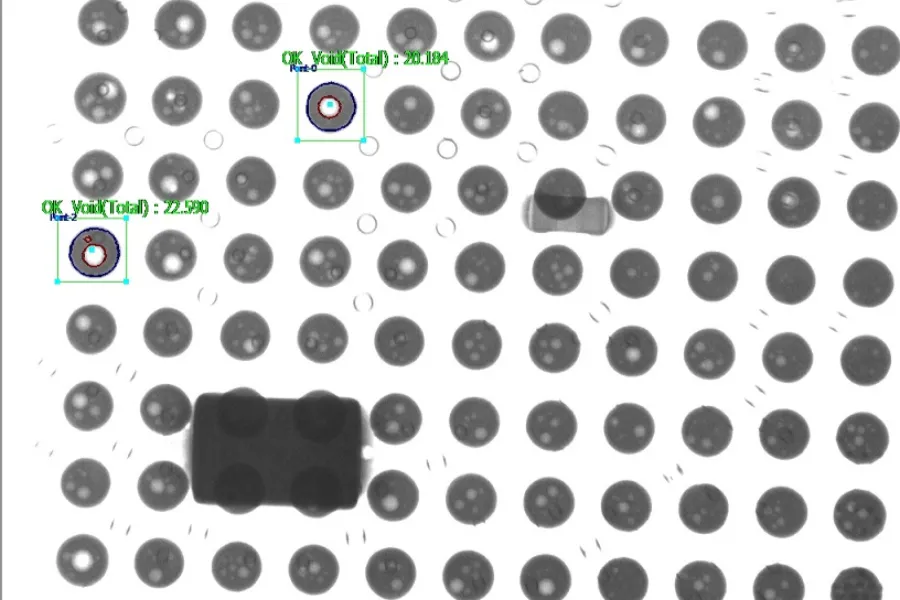
For multi-layered PCBs or boards with hidden solder joints, X-ray inspection for PCBs is a game-changer. This non-destructive PCB testing method uses X-ray radiation to penetrate the board and create detailed images of its internal structure. It’s particularly useful for inspecting ball grid array (BGA) components, where solder joints are hidden beneath the package and invisible to AOI or manual checks.
X-ray systems can reveal defects like voids in solder joints, which can compromise electrical connections and lead to failures. They can also detect misaligned vias, internal cracks, or insufficient solder paste in hidden areas. For example, a void larger than 25% of a solder joint’s area can weaken the connection, increasing the risk of thermal or mechanical failure. X-ray inspection helps catch these issues before they become problems.
There are two main types of X-ray inspection used in PCB quality control: 2D and 3D. 2D X-ray provides a flat image of the board, suitable for simpler assemblies, while 3D X-ray (also called computed tomography or CT) offers a detailed, three-dimensional view, ideal for complex, high-density boards. While X-ray systems are more expensive and slower than AOI, their ability to perform non-destructive testing on hidden features makes them indispensable.
Non-Destructive PCB Testing: Protecting Quality Without Damage
Both AOI and X-ray inspection fall under the umbrella of non-destructive PCB testing, meaning they evaluate the board without damaging it. This is a critical advantage over older methods like destructive testing, where boards were physically cut apart or stressed to failure to identify weaknesses. Non-destructive methods preserve the integrity of the PCB, allowing it to proceed to the next stage of production or be shipped to customers after inspection.
Other non-destructive techniques complementing AOI and X-ray include infrared (IR) imaging and acoustic microscopy. IR imaging detects heat anomalies caused by poor connections or short circuits, often identifying issues in live circuits under load. Acoustic microscopy uses sound waves to detect delamination or cracks within the PCB material, especially in laminated layers. These methods, while less common than AOI or X-ray, add another layer of assurance in defect detection for PCB imaging.
By combining multiple non-destructive testing methods, manufacturers can achieve near-perfect quality control. For instance, using AOI for surface defects, X-ray for internal issues, and IR for functional testing ensures comprehensive coverage, reducing defect rates to below 1% in many high-end production lines.
Defect Detection in PCB Imaging: Common Issues and Solutions
Defect detection in PCB imaging is all about identifying problems before they lead to failures. Let’s break down some of the most common defects and how advanced imaging techniques address them:
- Solder Joint Defects: Issues like voids, insufficient solder, or cold joints can disrupt electrical connectivity. X-ray inspection excels at spotting these hidden flaws, ensuring joints meet standards (e.g., void percentage below 25%).
- Component Misplacement: Even a slight misalignment of 0.05mm can cause connection issues. AOI systems catch these errors by comparing the board to design specifications with micron-level precision.
- Internal Cracks or Delamination: Cracks in vias or separation of PCB layers can lead to long-term reliability issues. X-ray CT and acoustic microscopy provide clear images of these internal defects without damaging the board.
- Short Circuits or Open Connections: These can result from excess solder or broken traces. AOI detects surface-level shorts, while X-ray and IR imaging help identify hidden or functional issues.
By leveraging the strengths of each imaging technique, manufacturers can address a wide range of defects, ensuring that only high-quality PCBs reach the market. This multi-layered approach to defect detection in PCB imaging is becoming the industry standard, especially for applications in automotive, aerospace, and medical devices where reliability is non-negotiable.
Benefits of Advanced PCB Imaging Techniques
Adopting advanced PCB quality control imaging offers numerous advantages for manufacturers and end-users alike. Here are some key benefits:
- Higher Accuracy: Technologies like AOI and X-ray achieve defect detection rates above 99%, far surpassing manual inspection.
- Cost Savings: Catching defects early reduces rework and scrap rates, saving up to 20-30% in production costs in high-volume settings.
- Faster Production: Automated systems like AOI speed up inspection without sacrificing quality, enabling manufacturers to meet tight deadlines.
- Improved Reliability: Non-destructive PCB testing ensures that hidden defects are identified, reducing field failures and enhancing product lifespan.
- Scalability: Advanced imaging systems can handle everything from small-batch prototypes to large-scale production, adapting to various board sizes and complexities.
These benefits make advanced imaging a worthwhile investment, especially as the demand for smaller, denser, and more reliable PCBs continues to grow.
Challenges and Considerations in PCB Quality Control Imaging
While advanced imaging techniques offer incredible value, they come with challenges that manufacturers must navigate. Equipment costs can be significant, with high-end X-ray systems running into hundreds of thousands of dollars. Additionally, operating these systems requires skilled technicians and regular maintenance to ensure accuracy.
Another consideration is the balance between inspection depth and production speed. While X-ray inspection provides unparalleled detail, it’s slower than AOI, potentially creating bottlenecks in high-speed lines. Manufacturers must strategically integrate these tools to optimize both quality and efficiency. For instance, using AOI for initial surface checks and reserving X-ray for critical boards or random sampling can strike the right balance.
Finally, data management is a growing concern. Advanced imaging systems generate vast amounts of data, from high-resolution images to defect logs. Storing, analyzing, and acting on this data requires robust software and infrastructure, adding another layer of complexity to the process.
Future Trends in PCB Imaging for Quality Control
The field of PCB quality control imaging is evolving rapidly, driven by advancements in artificial intelligence (AI) and machine learning (ML). These technologies are being integrated into AOI and X-ray systems to enhance defect detection capabilities. For example, AI algorithms can learn from past inspections to identify subtle patterns or anomalies that might be missed by traditional software, reducing false positives by up to 40%.
Another emerging trend is the use of real-time imaging and feedback loops. Future systems may provide instant defect analysis during assembly, allowing for immediate corrections rather than post-production rework. Additionally, as PCBs continue to shrink, imaging systems are being developed with higher resolutions and smaller focal points to inspect components at the nanoscale level.
These innovations promise to make PCB imaging even more precise and efficient, ensuring that quality control keeps pace with the ever-increasing complexity of electronic devices.
Conclusion: Elevating PCB Quality with Advanced Imaging
In the world of PCB manufacturing, quality control is non-negotiable. While visual inspection once sufficed, the complexity of modern electronics demands more sophisticated solutions. Advanced PCB imaging techniques like automated optical inspection (AOI), X-ray inspection for PCBs, and other non-destructive PCB testing methods provide the precision and reliability needed to catch defects early and ensure flawless products.
By embracing these technologies, manufacturers can achieve higher accuracy, reduce costs, and deliver PCBs that meet the stringent demands of industries like automotive, medical, and consumer electronics. As innovations like AI and real-time imaging continue to shape the future, the potential for defect detection in PCB imaging will only grow, paving the way for even better quality control.


