 ALLPCB


If you're dealing with high-speed printed circuit boards (PCBs), back drilling is a critical process to ensure optimal performance. However, PCB back drilling errors can lead to signal integrity issues, increased manufacturing costs, and project delays. In this blog, we'll uncover the top 5 back drilling mistakes to avoid, helping you maintain signal integrity, manage via stub length, and prevent controlled depth drilling problems. Whether you're an engineer or a PCB designer, this guide offers practical insights to enhance your designs and manufacturing processes.
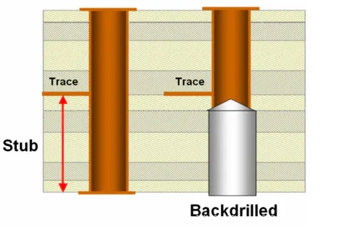
Back drilling is a technique used to remove unused portions of plated-through holes (PTHs) in multilayer PCBs, reducing via stubs that can degrade signal quality. While the process sounds straightforward, small errors can have significant consequences. Let's dive into the common pitfalls and how to sidestep them for better PCB performance.
What Is Back Drilling and Why Does It Matter?
Before we explore the mistakes, let's clarify what back drilling entails. Back drilling is a manufacturing process where a slightly larger drill bit is used to remove the conductive stub of a via from the opposite side of the PCB after the initial drilling and plating. This stub, if left intact, can act as an antenna, causing signal reflections and degrading signal integrity, especially in high-speed designs operating at frequencies above 1 GHz.
The primary goal of back drilling is to minimize via stub length. A long stub can introduce impedance mismatches, leading to signal loss or distortion. For instance, in a 10-layer PCB with a signal transitioning from layer 2 to layer 8, the unused via stub extending to layer 10 can cause a reflection, impacting data rates as high as 10 Gbps. By removing this stub, back drilling ensures cleaner signal transmission, which is vital for applications like telecommunications, data centers, and advanced computing.
Mistake 1: Incorrect Via Stub Length Calculation
One of the most frequent back drilling mistakes is miscalculating the via stub length that needs to be removed. The stub length directly affects signal integrity, as longer stubs increase the risk of signal reflections. For high-speed signals, even a stub length of 0.010 inches (0.25 mm) can cause noticeable degradation at frequencies above 5 GHz.
To avoid this error, use simulation tools to model the via stub's impact on impedance and signal loss. Ensure that the stub length after back drilling is less than one-tenth of the wavelength of the highest frequency signal. For example, at 10 GHz, the wavelength in a typical FR-4 material (with a dielectric constant of 4.2) is about 0.59 inches (15 mm), so the stub should ideally be shorter than 0.059 inches (1.5 mm).
Additionally, communicate precise stub length requirements to your manufacturer. Without clear specifications, the drilling depth may be inconsistent, leaving behind stubs that still interfere with signals. Always double-check design files to confirm that the stub length aligns with your performance goals.
Mistake 2: Poor Controlled Depth Drilling Precision
Another common issue is inadequate precision in controlled depth drilling. Back drilling requires exact control over the drill depth to remove the via stub without damaging the active signal layers. Controlled depth drilling problems can occur if the drilling equipment isn't calibrated correctly or if the PCB stack-up data is inaccurate.
For instance, if a drill overshoots by just 0.005 inches (0.13 mm), it could cut into a critical signal layer, causing an open circuit or short. Conversely, under-drilling leaves a longer stub, negating the purpose of back drilling. Modern PCB designs often have tight tolerances, with layer thicknesses as thin as 0.002 inches (0.05 mm), making precision non-negotiable.
To prevent this, ensure that your manufacturing partner uses advanced drilling machines with depth control accuracy within 0.001 inches (0.025 mm). Provide detailed stack-up information, including layer thicknesses and dielectric constants, to avoid miscalculations. Testing a prototype board before full production can also help identify and correct depth-related issues early on.
Mistake 3: Ignoring Signal Integrity During Design
Many signal integrity problems arise because designers overlook the impact of vias and stubs during the initial PCB layout. Back drilling is often treated as an afterthought rather than a core part of the design process. This can lead to vias placed in suboptimal locations or designs that don't account for the need for back drilling at all.
For high-speed signals, vias should be placed to minimize stub length from the start. If a signal transitions between inner layers, ensure the via extends only to the necessary depth, reducing the stub that needs to be drilled out later. Additionally, simulate the design to predict signal reflections and impedance mismatches. Tools like 3D electromagnetic solvers can estimate how a stub affects a signal's rise time, which for a 10 Gbps signal might degrade from 35 ps to 50 ps due to reflections.
Work closely with your design team to integrate back drilling requirements into the layout phase. Specify which vias need back drilling and verify that the design rules account for signal integrity constraints. By planning ahead, you can reduce costly redesigns and manufacturing errors.
Mistake 4: Overlooking Material and Tooling Compatibility
Not all PCB materials and drilling tools are suited for back drilling, and failing to account for this can lead to PCB back drilling errors. For example, harder materials like high-Tg laminates or ceramics can wear out drill bits faster, causing inconsistent hole sizes or depths. Similarly, using a drill bit that's too large or too small compared to the via diameter can result in incomplete stub removal or damage to the via barrel.
Standard FR-4 material, with a glass transition temperature (Tg) of around 130°C, is generally compatible with back drilling, but high-frequency materials like Rogers 4350B (Tg of 280°C) may require specialized tools. The drill bit diameter should typically be 0.002 to 0.004 inches (0.05 to 0.1 mm) larger than the via to ensure complete stub removal without affecting the plated barrel.
To avoid issues, select materials and tooling that match the requirements of your design. Consult with your manufacturer to confirm that their equipment can handle the chosen materials and that their processes are optimized for back drilling. Regularly maintaining and replacing drill bits can also prevent errors caused by wear and tear.
Mistake 5: Failing to Test and Validate Post-Drilling
Even with a well-planned design and precise manufacturing, skipping post-drilling validation can introduce unnoticed back drilling mistakes. Without proper testing, issues like incomplete stub removal or accidental damage to signal layers might go undetected until the PCB fails in operation. This can be disastrous for high-speed applications where signal integrity is paramount.
After back drilling, use techniques like Time Domain Reflectometry (TDR) to measure impedance discontinuities caused by remaining stubs. A TDR test can reveal if a stub is causing a reflection, with impedance mismatches as small as 5 ohms indicating a problem. Additionally, cross-sectioning a sample board under a microscope can visually confirm whether the stub has been removed to the correct depth.
Incorporate validation steps into your quality assurance process. Test a few boards from each batch to ensure consistency, and use the data to refine future designs. This proactive approach can save time and resources by catching errors before they escalate into larger issues.
Best Practices for Successful Back Drilling
Now that we've covered the common mistakes, here are some actionable tips to ensure successful back drilling and avoid controlled depth drilling problems:
- Collaborate Early: Work with your manufacturer during the design phase to align on back drilling requirements and capabilities.
- Use Advanced Tools: Leverage simulation software to predict and mitigate signal integrity problems before manufacturing.
- Specify Tolerances: Clearly define drilling depth and stub length tolerances in your design files to prevent miscommunication.
- Choose the Right Partner: Select a manufacturing service with proven expertise in back drilling for high-speed PCBs.
- Iterate and Improve: Use feedback from testing to continuously refine your back drilling processes and designs.
Conclusion: Mastering Back Drilling for High-Performance PCBs
Back drilling is a powerful technique to enhance the performance of high-speed PCBs, but it comes with challenges that can impact signal integrity if not handled carefully. By avoiding these five common PCB back drilling errors—miscalculating via stub length, lacking precision in controlled depth drilling, ignoring signal integrity in design, overlooking material compatibility, and skipping post-drilling validation—you can achieve cleaner signal transmission and more reliable boards.
Implementing the best practices outlined in this guide will help you navigate the complexities of back drilling and deliver high-quality PCBs for demanding applications. With careful planning, precise execution, and thorough testing, you can minimize back drilling mistakes and ensure your designs perform at their best.
At ALLPCB, we're committed to supporting engineers and designers with the tools and expertise needed for successful PCB manufacturing. Whether you're tackling high-speed designs or complex multilayer boards, mastering back drilling is a step toward excellence in your projects.


