 ALLPCB


If you're searching for effective ways to improve PCB reliability, microsectioning is a powerful tool in failure analysis that can uncover hidden defects and root causes of issues. This technique, often called cross-sectioning, allows engineers to inspect the internal structure of a printed circuit board (PCB) to identify manufacturing flaws and ensure quality. In this blog, we'll explore how microsectioning works, why it’s critical for root cause analysis, and how it helps in identifying PCB manufacturing defects. Let’s dive into the details of PCB failure analysis methods and see how this process can elevate your board’s performance and durability.
What Is Microsectioning and Why Does It Matter for PCB Reliability?
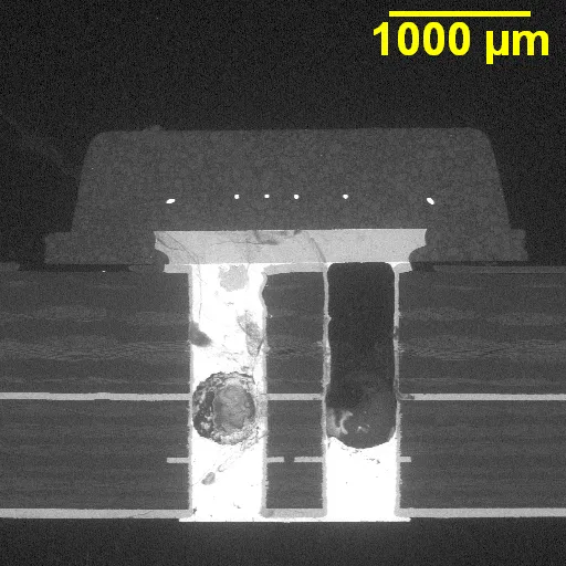
Microsectioning is a destructive testing method used in PCB failure analysis to examine the internal layers and structures of a board. By cutting a small section of the PCB and preparing it for microscopic inspection, engineers can reveal issues that are not visible on the surface. This process is essential for identifying problems like poor plating, delamination, or cracks that could lead to circuit failures.
Why does this matter? PCBs are the backbone of electronic devices, and even a tiny defect can cause significant issues, such as signal loss or complete system failure. For instance, a crack in a via might disrupt a signal path, leading to impedance mismatches (often in the range of 50-100 ohms for high-speed designs). By using microsectioning, you can catch these defects early, preventing costly recalls or field failures. This method is a cornerstone of PCB failure analysis methods, ensuring that boards meet strict quality standards.
How Microsectioning Works: A Step-by-Step Guide
Microsectioning for root cause analysis involves a systematic process to prepare and analyze a PCB sample. Here’s how it typically works:
- Sample Selection: Choose a specific area of the PCB suspected of having defects or a representative section for overall quality checks.
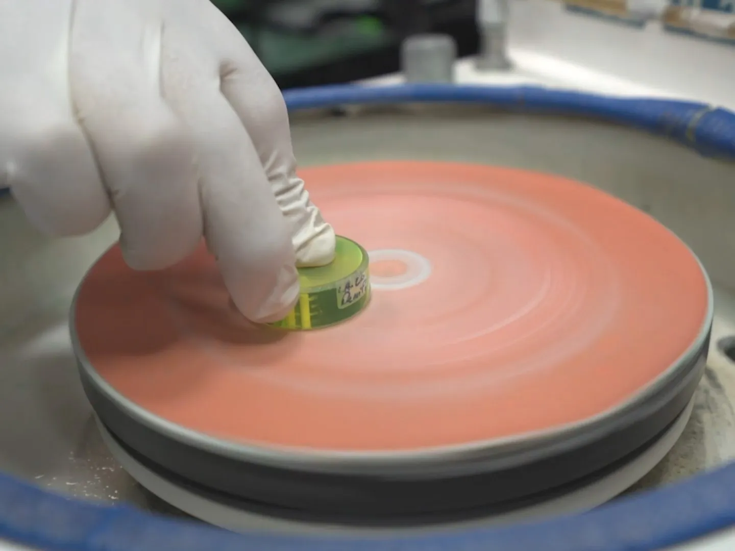
- Cutting: Use precision tools to cut a small piece of the board without damaging the internal structures. This often involves a diamond saw or similar equipment to ensure clean edges.
- Mounting: Embed the cut sample in a resin or epoxy material to stabilize it for further processing.
- Grinding and Polishing: Gradually grind and polish the sample to expose the internal layers and features, achieving a smooth surface for clear microscopic viewing.
- Inspection: Examine the prepared sample under a high-powered microscope (often at magnifications of 50x to 1000x) to identify defects like voids in solder joints, insufficient copper plating (which should ideally be 25-50 micrometers thick for standard vias), or interlayer misalignment.
- Documentation: Record findings with detailed images and measurements to support root cause analysis and inform corrective actions.
This meticulous process ensures that even the smallest flaws, such as a hairline crack measuring less than 10 micrometers, are detected. These insights are invaluable for improving manufacturing processes and preventing future issues.
Common PCB Manufacturing Defects Uncovered by Microsectioning
Identifying PCB manufacturing defects is a primary goal of microsectioning. This technique can reveal a wide range of issues that affect board reliability. Here are some common defects it helps uncover:
- Plating Voids: Incomplete copper plating in vias or through-holes can lead to weak electrical connections. Microsectioning can show if the plating thickness falls below the industry standard of 20-25 micrometers, indicating a potential failure point.
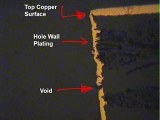
- Delamination: Separation between PCB layers due to poor bonding or thermal stress can disrupt signal integrity. Cross-section analysis often reveals gaps or bubbles between layers.
- Cracks: Micro-cracks in vias, pads, or traces (sometimes as small as 5 micrometers) can form due to mechanical stress or thermal cycling. These are often invisible on the surface but clear under a microscope.
- Solder Joint Issues: Poor soldering, such as insufficient wetting or voids, can cause intermittent connections. Microsectioning exposes these flaws for detailed analysis.
- Resin Smearing: During drilling, resin from the PCB substrate can smear over copper layers, affecting conductivity. This defect is easily spotted in a cross-section view.
By pinpointing these issues, microsectioning provides actionable data to refine manufacturing processes, ensuring that boards withstand operational stresses like thermal cycles ranging from -40°C to 85°C in typical industrial applications.
Why Microsectioning Is Essential for Root Cause Analysis
Microsectioning for root cause analysis goes beyond just identifying defects—it helps determine why they occurred in the first place. Understanding the root cause is critical for preventing recurring issues and improving overall PCB quality. Here’s why this method stands out among PCB failure analysis methods:
- Internal Visibility: Unlike surface-level inspections, microsectioning provides a direct view of internal structures, revealing hidden problems that other methods might miss.
- Precise Measurements: Engineers can measure exact dimensions, such as the thickness of copper layers or the depth of cracks, to assess compliance with design specifications. For example, a via barrel should ideally have a uniform copper thickness of around 25 micrometers.
- Correlation with Failure Modes: By comparing microsection findings with electrical test results (like continuity checks showing open circuits), engineers can link specific defects to performance issues, such as a signal delay caused by a broken trace.
- Process Improvement: Insights from microsectioning often point to specific manufacturing steps needing adjustment, such as optimizing drilling speeds (typically 50,000-100,000 RPM) to avoid resin smearing.
This detailed analysis ensures that every aspect of the PCB, from material quality to assembly techniques, is scrutinized and optimized for reliability.
Integrating Microsectioning into Your Quality Control Process
To maximize the benefits of microsectioning, it’s important to integrate it strategically into your quality control workflow. Here are some practical tips for making this method a regular part of your PCB failure analysis methods:
- Schedule Routine Checks: Perform microsectioning on a small percentage of boards (e.g., 1-2% of each batch) to monitor consistent quality without significantly increasing costs.
- Prioritize High-Risk Areas: Focus on sections of the PCB most prone to defects, such as densely populated via regions or areas exposed to high thermal stress.
- Use Advanced Tools: Invest in high-resolution microscopes and precision cutting equipment to ensure accurate results. Modern microscopes with digital imaging can capture defects at resolutions down to 1 micrometer.
- Train Your Team: Ensure that engineers and technicians are skilled in preparing and analyzing microsections to avoid errors like over-grinding, which can obscure critical details.
- Document and Analyze Trends: Maintain a database of microsection findings to track recurring defects and correlate them with specific manufacturing conditions, such as humidity levels during lamination (ideally kept below 50%).
By embedding microsectioning into your process, you create a proactive approach to quality control, catching issues before they escalate into widespread failures.
Challenges and Limitations of Microsectioning
While microsectioning is a powerful tool, it’s not without challenges. Understanding these limitations helps set realistic expectations and complements this method with other PCB failure analysis methods.
- Destructive Nature: Since microsectioning involves cutting the PCB, the tested sample cannot be reused. This can be a drawback when dealing with expensive or limited-production boards.
- Time-Intensive: Preparing and analyzing a microsection can take several hours, making it less suitable for rapid assessments during high-volume production.
- Localized Analysis: Microsectioning only examines a specific area of the board, so defects in other regions might go undetected unless multiple samples are taken.
- Skill Dependency: The accuracy of results heavily relies on the operator’s expertise. Improper preparation, such as uneven polishing, can lead to misleading observations.
Despite these challenges, the depth of insight provided by microsectioning often outweighs the drawbacks, especially for critical applications where reliability is non-negotiable, such as in aerospace or medical devices with strict signal integrity requirements (e.g., maintaining differential pair impedance within ±10% of 100 ohms).
Complementing Microsectioning with Other Failure Analysis Methods
To build a comprehensive failure analysis strategy, microsectioning should be paired with non-destructive testing methods. This combination ensures a thorough evaluation of PCB reliability. Here are a few complementary techniques:
- X-Ray Inspection: Ideal for detecting internal voids or misalignments without cutting the board. It’s especially useful for inspecting ball grid array (BGA) components.
- Thermal Imaging: Identifies hot spots on the PCB that may indicate short circuits or high-resistance areas, often operating at temperatures exceeding 100°C under load.
- Electrical Testing: Measures parameters like continuity and insulation resistance to pinpoint electrical failures, often detecting open circuits with resistances above 1 megaohm.
- Acoustic Microscopy: Uses sound waves to detect delamination or cracks, providing a non-destructive alternative for internal defect analysis.
By combining these methods with microsectioning, you gain a complete picture of the PCB’s condition, ensuring no defect goes unnoticed.
Conclusion: Harnessing Microsectioning for Unmatched PCB Reliability
Microsectioning is a game-changer in the realm of PCB failure analysis methods, offering unparalleled insight into the internal structure of boards. By enabling precise identification of manufacturing defects and supporting root cause analysis, this technique helps engineers ensure that PCBs meet the highest standards of reliability. From detecting plating voids to uncovering delamination, microsectioning for root cause analysis empowers manufacturers to address issues at their source, reducing the risk of failures in the field.
Integrating this method into your quality control process, while complementing it with other testing techniques, creates a robust framework for producing durable, high-performance PCBs. Whether you’re dealing with high-speed designs requiring tight impedance control or rugged boards for harsh environments, microsectioning provides the clarity needed to achieve excellence. Start leveraging this powerful tool today to unlock the full potential of your PCB designs and deliver products that stand the test of time.


