 ALLPCB


In PCB manufacturing, the minimum line width plays a critical role in balancing cost and performance. Simply put, smaller line widths allow for denser designs and better signal integrity, but they often increase production costs due to tighter tolerances and advanced fabrication techniques. On the other hand, wider lines are cheaper to produce but may compromise performance in high-speed or compact circuits. In this detailed guide, we’ll explore how minimum line width impacts PCB manufacturing cost, trace width considerations, and overall performance, helping you make informed decisions for your next project.
What is Minimum Line Width in PCB Manufacturing?
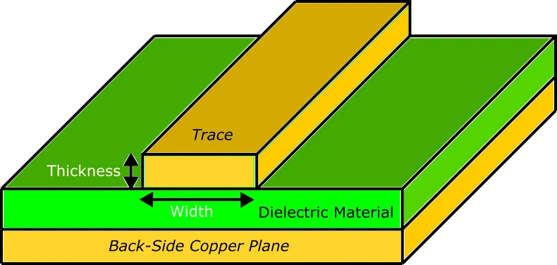
Minimum line width refers to the smallest width of a conductive trace that a PCB manufacturer can reliably produce on a circuit board. This measurement, often expressed in mils (1 mil = 0.001 inches) or micrometers (μm), is a key factor in determining the density and complexity of a PCB design. Common minimum line widths in standard manufacturing range from 6 mils (0.152 mm) to 3 mils (0.076 mm), though advanced processes can achieve even smaller traces down to 2 mils or below for high-density interconnect (HDI) boards.
Understanding minimum line width is essential because it directly affects both the cost of fabrication and the performance of the final product. Let’s dive deeper into these aspects to see how trace width ties into PCB fabrication tolerances and pricing.
Why Minimum Line Width Matters
The line width of traces on a PCB influences several critical factors:
- Signal Integrity: Narrower traces can reduce parasitic capacitance and improve high-frequency performance, which is vital for applications like 5G or high-speed digital circuits.
- Current Carrying Capacity: Wider traces can handle higher currents without overheating, making them ideal for power circuits.
- Manufacturing Cost: Smaller line widths require precision equipment and tighter tolerances, driving up the price of production.
- Design Density: Thinner traces allow for more compact layouts, enabling smaller devices with more components in a limited space.
PCB Manufacturing Cost and Trace Width: Breaking Down the Relationship
When it comes to PCB manufacturing cost, trace width is a significant factor. Manufacturers must use specialized equipment and processes to achieve smaller line widths, which directly impacts the price of production. Let’s explore how minimum line width affects cost and what you can expect when budgeting for your PCB project.
Cost Implications of Smaller Line Widths
Producing PCBs with smaller line widths requires advanced technology, such as high-precision photolithography and etching processes. Here are some reasons why costs increase with narrower traces:
- Tighter Fabrication Tolerances: Achieving a minimum line width of 3 mils or less demands stricter control over the etching process, which increases the risk of defects and requires more rigorous quality checks.
- Specialized Materials: High-density designs often need thinner copper layers or specialized substrates to maintain signal integrity, adding to material costs.
- Advanced Equipment: Smaller traces may require laser direct imaging (LDI) instead of traditional photomasks, which is more expensive but offers greater precision.
- Lower Yields: The smaller the line width, the higher the chance of manufacturing errors, leading to lower yields and higher costs per usable board.
For example, a standard PCB with a minimum line width of 6 mils might cost $0.50 per square inch for a double-layer board in moderate volumes. However, reducing the line width to 3 mils could increase the cost to $1.00 or more per square inch due to the need for advanced processes. These numbers can vary based on volume, board complexity, and other design factors, but they illustrate the cost trend associated with PCB fabrication tolerances for line width.
Balancing Cost with Design Needs
To manage costs, it’s important to align the minimum line width with the actual requirements of your project. For instance, if your design operates at low frequencies (below 100 MHz), wider traces of 6-8 mils might suffice, keeping production costs low. However, for high-speed applications exceeding 1 GHz, narrower traces of 3-4 mils may be necessary to minimize signal loss and crosstalk, even if it means a higher PCB manufacturing cost for trace width.
Performance Analysis: How Line Width Affects PCB Functionality
Beyond cost, the minimum line width has a profound impact on the performance of a PCB. Whether you’re designing for power delivery, signal integrity, or thermal management, understanding these effects is crucial for optimizing your board.
Signal Integrity and Impedance Control
In high-speed circuits, trace width directly affects impedance, which must be controlled to ensure reliable signal transmission. For example, a typical 50-ohm impedance for RF signals might require a trace width of 4 mils on a standard 1.6 mm FR-4 substrate with a dielectric constant of 4.2. If the trace width deviates even slightly due to manufacturing tolerances, it can lead to impedance mismatch, causing signal reflections and data errors.
Narrower traces also reduce parasitic capacitance between adjacent lines, which is beneficial for minimizing crosstalk in high-density designs. However, if the traces are too narrow, they may introduce higher resistance, leading to signal attenuation over long distances.
Current Carrying Capacity
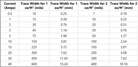
For power circuits, wider traces are essential to handle higher currents without excessive heating. A trace width of 10 mils might safely carry 1 ampere of current at a copper thickness of 1 oz/ft2, but reducing the width to 5 mils could limit the current to 0.5 amperes under the same conditions, risking overheating and potential failure. Tools like trace width calculators can help determine the optimal width based on current, temperature rise, and copper thickness.
Thermal Management
Trace width also influences how heat dissipates in a PCB. Wider traces can act as heat sinks, spreading thermal energy more effectively than narrow ones. In designs where components generate significant heat, using wider traces in critical areas can prevent hotspots and improve reliability.
PCB Fabrication Tolerances and Line Width: What to Expect
PCB fabrication tolerances for line width refer to the acceptable variation in trace width during manufacturing. These tolerances are critical because even small deviations can affect performance, especially in high-speed or high-density designs. Let’s look at what influences these tolerances and how they tie into minimum line width PCB price.
Standard Tolerances in PCB Manufacturing
For most standard PCB processes, manufacturers guarantee a tolerance of ±10% on trace widths. For a 6-mil trace, this means the actual width could range from 5.4 to 6.6 mils. However, as the minimum line width decreases, maintaining tight tolerances becomes more challenging. For a 3-mil trace, the same ±10% tolerance results in a range of 2.7 to 3.3 mils, but achieving this precision often requires advanced fabrication techniques, increasing costs.
Factors Affecting Fabrication Tolerances
Several factors influence how tightly a manufacturer can control line width:
- Etching Process: Wet etching, a common method, can undercut traces, leading to wider variations. More advanced dry etching or laser processes offer better control but at a higher cost.
- Copper Thickness: Thicker copper layers (e.g., 2 oz/ft2) are harder to etch precisely compared to thinner layers (e.g., 0.5 oz/ft2), affecting tolerance.
- Design Complexity: High-density designs with closely spaced traces are more prone to manufacturing variations, requiring stricter process controls.
To minimize issues with tolerances, it’s wise to consult with your manufacturing partner early in the design phase. Providing a design with slightly wider traces than the absolute minimum can also reduce the risk of performance issues due to fabrication variations, potentially lowering the minimum line width PCB price.
Practical Tips for Choosing the Right Minimum Line Width
Selecting the appropriate minimum line width for your PCB design involves balancing cost, performance, and manufacturability. Here are some actionable tips to guide your decision:
- Assess Performance Needs: Determine the frequency, current, and density requirements of your circuit. For low-speed designs, wider traces (6-8 mils) are often sufficient and cost-effective. For high-speed or compact designs, consider narrower traces (3-4 mils) despite the higher cost.
- Use Design Tools: Leverage trace width calculators to estimate the optimal width based on current, impedance, and thermal constraints. Many online tools are available to simplify this process.
- Communicate with Manufacturers: Early collaboration with your PCB fabricator can help you understand their capabilities and tolerances, ensuring your design aligns with their process limits.
- Plan for Scalability: If you anticipate future iterations or higher production volumes, choose a line width that balances cost and performance to avoid costly redesigns later.
Conclusion: Striking the Right Balance in PCB Design
The minimum line width in PCB manufacturing is a pivotal factor that influences both cost and performance. Smaller line widths enable denser, high-performance designs but come with higher production costs due to tighter tolerances and advanced processes. Wider traces, while more affordable, may not meet the demands of modern high-speed or compact applications. By carefully evaluating your project’s requirements—such as signal integrity, current capacity, and budget—you can select the optimal trace width to achieve the best balance.
Understanding PCB fabrication tolerances for line width and working closely with your manufacturing partner can further ensure a successful outcome. Whether you’re aiming to minimize PCB manufacturing cost for trace width or optimize performance, a well-informed approach to line width selection will set your project up for success.


