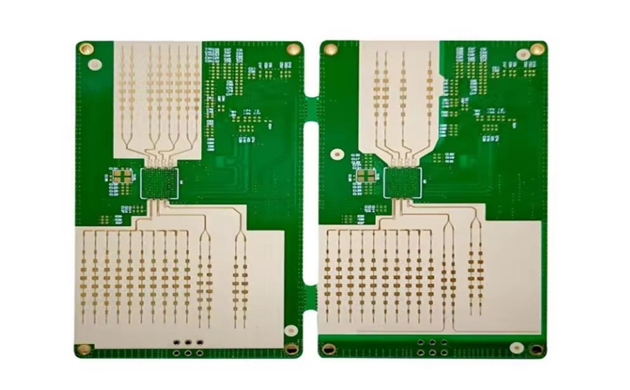
Are you a hobbyist eager to dive into your first multi-layer PCB project? Multi-layer PCB design might sound complex, but with the right guidance, it’s an achievable and rewarding step in DIY electronics projects. In this guide, we’ll walk you through an easy multi-layer PCB design process tailored for beginners. From understanding the basics to creating a simple PCB layout, we’ve got you covered with practical tips and clear steps to help you succeed in your beginner PCB design journey.
Whether you’re building a small gadget or experimenting with circuits, this blog will break down everything you need to know about designing your first multi-layer PCB. Let’s get started on this exciting path to creating functional and efficient electronics!
What Is a Multi-Layer PCB and Why Use It for Your First Project?
A multi-layer PCB (Printed Circuit Board) is a board with more than two layers of conductive material, typically copper, separated by insulating layers. Unlike single or double-layer boards, multi-layer PCBs allow for more complex circuits in a smaller space by stacking layers. This makes them ideal for compact, high-performance projects.
For hobbyists tackling their first multi-layer PCB project, these boards offer several benefits. They can handle denser circuits, reduce noise in signals, and improve overall performance for devices like microcontrollers or sensors. While they might seem intimidating, starting with a simple design can be an excellent learning experience in DIY electronics projects.
Key Advantages of Multi-Layer PCBs for Beginners
- Space Efficiency: Stack multiple layers to fit more components in a smaller footprint, perfect for compact gadgets.
- Better Signal Integrity: Separate power and ground planes reduce interference, ensuring cleaner signals (e.g., minimizing crosstalk by up to 20% in some designs).
- Learning Opportunity: Working on an easy multi-layer PCB design teaches advanced skills that can be applied to future projects.
Suggested Image Placement: Insert an image here showing a cross-section of a multi-layer PCB with labeled layers (e.g., top layer, ground plane, inner layers). ALT Text: "Cross-section of a multi-layer PCB showing stacked layers for beginner PCB design."
Getting Started: Tools and Materials for Your First Multi-Layer PCB Project
Before diving into your first multi-layer PCB project, gather the necessary tools and materials. As a hobbyist, you don’t need expensive equipment to start. Focus on accessible software and basic components to keep your beginner PCB design journey smooth and cost-effective.
Essential Tools for Easy Multi-Layer PCB Design
- Design Software: Use free or affordable PCB design tools that support multi-layer layouts. Look for beginner-friendly options with tutorials to help you create a simple PCB layout.
- Computer with Decent Specs: Ensure your device can run design software smoothly for schematic and layout work.
- Basic Electronics Kit: Gather resistors, capacitors, LEDs, and a microcontroller (like an Arduino-compatible board) for a simple test project.
Materials for DIY Electronics Projects
- PCB Prototyping Service: Partner with a reliable manufacturer to produce your multi-layer board. Many offer low-cost options for small runs, perfect for hobbyists.
- Soldering Tools: A soldering iron, solder, and a multimeter will help you assemble and test your board after fabrication.
Step-by-Step Guide to Designing Your First Multi-Layer PCB
Designing a multi-layer PCB as a beginner might feel daunting, but breaking it down into manageable steps makes it approachable. Follow this guide to create a simple PCB layout for your DIY electronics project. We’ll focus on a basic 4-layer design, which is a common starting point for hobbyists.
Step 1: Define Your Project Goal
Start by deciding what your first multi-layer PCB project will do. For beginners, a simple circuit like an LED controller with a microcontroller is a great choice. Keep the component count low (e.g., under 20 components) to avoid complexity. Define inputs, outputs, and power requirements (e.g., 5V DC for a small microcontroller setup).
Step 2: Create a Schematic
Using your chosen design software, draw a schematic of your circuit. This is like a blueprint showing how components connect. For a 4-layer PCB, plan to separate power and ground on dedicated layers to reduce noise. Ensure all connections are correct before moving to the layout phase.
Step 3: Plan Your Layer Stack-Up
In a 4-layer PCB, a common stack-up for hobbyists is:
- Layer 1 (Top): Signal traces and components.
- Layer 2: Ground plane to shield signals and reduce noise.
- Layer 3: Power plane for consistent voltage distribution.
- Layer 4 (Bottom): Additional signal traces or secondary ground.
This setup minimizes interference and keeps impedance controlled (e.g., maintaining a 50-ohm impedance for high-speed signals if needed). Keep critical traces short to avoid delays (signal speed can degrade over long distances at rates of about 6 inches per nanosecond in FR-4 material).
Step 4: Design the Layout
Switch to the layout editor in your software to place components and route traces. Follow these tips for an easy multi-layer PCB design:
- Place components logically, grouping related parts (e.g., microcontroller near supporting capacitors).
- Route high-speed signals on the top layer, avoiding crossings with power lines.
- Use vias (small holes) to connect traces between layers, but keep them minimal to reduce fabrication costs.
Step 5: Run Design Rule Checks (DRC)
Most software includes a DRC tool to check for errors like overlapping traces or insufficient spacing. For beginners, maintain at least 6 mils (0.006 inches) between traces to prevent short circuits during manufacturing. Fix any issues before finalizing your design.
Step 6: Generate Gerber Files and Order Your PCB
Once your design is error-free, export Gerber files—the standard format for PCB manufacturing. Upload these files to a fabrication service to order your board. Many services offer quick turnaround for small batches (e.g., 5 boards for under $20 for simple designs), making it affordable for hobbyists.
Tips for Success in Beginner PCB Design
As you work on your first multi-layer PCB project, keep these practical tips in mind to ensure a smooth process and a functional result.
- Start Small: Choose a project with minimal layers (e.g., 4 layers) and fewer components to learn the basics without feeling overwhelmed.
- Learn Layer Separation: Dedicate layers to specific functions (like power and ground) to improve performance and reduce noise by up to 15% compared to mixed layers.
- Test Incrementally: After receiving your board, solder and test one section at a time (e.g., power supply first) to catch issues early.
- Use Online Resources: Watch tutorials or read forums for advice on easy multi-layer PCB design challenges like routing or via placement.
Common Challenges in Multi-Layer PCB Design and How to Overcome Them
Even with a simple PCB layout, hobbyists often face hurdles in multi-layer designs. Here are some common issues and solutions to keep your project on track.
Challenge 1: Signal Interference
In multi-layer boards, signals can interfere if traces are too close. To fix this, maintain a ground plane between signal layers to shield them. Aim for at least 10 mils of separation between high-speed traces to keep crosstalk below 5%.
Challenge 2: Overcomplicated Routing
Beginners might overcomplicate trace routing, leading to delays or errors. Stick to straight, short paths and use auto-routing features in software for initial layouts, then manually adjust for optimization.
Challenge 3: Cost Concerns
Multi-layer PCBs can be pricier than single-layer ones. To save money, design smaller boards (e.g., under 50mm x 50mm) and order in small quantities during initial tests.
Ideas for Simple Multi-Layer PCB Projects for Hobbyists
If you’re unsure where to start, here are a few beginner-friendly DIY electronics projects that work well with a multi-layer PCB design.
- LED Matrix Display: Build a small display with a microcontroller to control LEDs. Use a 4-layer board to separate power, ground, and signal layers for clarity.
- Temperature Sensor Module: Create a circuit with a sensor and display to show temperature readings. A multi-layer design ensures stable power delivery for accurate data.
- Simple Audio Amplifier: Design a compact amplifier for a speaker. Multi-layer boards help reduce noise in audio signals for clearer sound output.
Why Choose Multi-Layer PCBs for Future DIY Electronics Projects?
Once you’ve completed your first multi-layer PCB project, you’ll likely see the value in using this approach for future designs. Multi-layer boards open doors to more advanced projects by offering better performance and flexibility. They allow you to experiment with high-speed circuits (e.g., signals up to 100 MHz with controlled impedance) and integrate more features into smaller devices.
By mastering an easy multi-layer PCB design now, you’re setting yourself up for success in creating innovative gadgets, from smart home devices to wearable tech. The skills you gain—like layer planning and noise reduction—will be invaluable as you grow as a hobbyist.
Final Thoughts on Beginner PCB Design
Designing your first multi-layer PCB project is a fantastic way to level up your skills in DIY electronics projects. While it may seem challenging at first, starting with a simple PCB layout and following a structured process makes it manageable and fun. From planning your layer stack-up to soldering your final board, each step teaches you something new about electronics design.
Remember to keep your initial designs straightforward, use the right tools, and learn from any mistakes along the way. With patience and practice, your beginner PCB design journey will lead to impressive creations. Dive in today, and let your creativity shine through your first multi-layer PCB!
 ALLPCB


