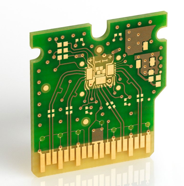
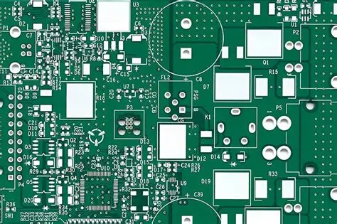
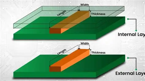
Printed circuit boards are the backbone of modern electronics. As technology advances and devices become smaller and more powerful, the demand for high-performance PCBs has increased significantly. Two major categories of PCBs dominate the market today: High-Density Interconnect (HDI) PCBs and standard multilayer PCBs. Both types have their own advantages and specific applications, and understanding the differences between them is critical for choosing the right solution for your project.
What is a Standard Multilayer PCB?
A standard multilayer PCB consists of three or more layers of conductive copper foil and insulating material laminated together. These layers are interconnected through drilled holes known as vias. Multilayer PCBs are widely used in electronics due to their ability to support complex circuits within a compact form factor.
Key Features of Standard Multilayer PCBs:
- Typically 4 to 12 layers, though more are possible
- Uses through-hole vias for interconnections
- Suitable for medium-complexity designs
- Cost-effective and widely available
Multilayer PCBs are common in applications such as consumer electronics, industrial equipment, automotive systems, and more. They provide an excellent balance between complexity, cost, and performance.
What is an HDI PCB?
High-Density Interconnect (HDI) PCBs are a more advanced type of circuit board that allows for a higher wiring density per unit area. This is achieved through the use of microvias, blind and buried vias, and fine line widths and spaces. HDI technology enables designers to create smaller, lighter, and more reliable products.
Key Features of HDI PCBs:
- High wiring density with finer trace widths
- Utilizes microvias, blind vias, and buried vias
- Supports higher layer counts with thinner substrates
- Enables advanced functionality in smaller form factors
HDI PCBs are commonly used in smartphones, tablets, medical devices, military and aerospace systems, and other high-performance applications where space and weight are critical constraints.
HDI Structures
1+N+1 - PCBs contain 1 'build-up' of high-density interconnection layers.
i+N+i (i≥2) - PCBs contain 2 or more 'build-up' of high density interconnection layers. Microvias on different layers can be staggered or stacked. Copper filled stacked microvia structures are commonly seen in demanding designs.
Main Differences
1. Layer Construction and Density
Standard Multilayer: Uses through-hole vias; lower layer density.
HDI: Uses microvias, blind/buried vias; higher layer density and finer features.
2. Size and Weight
Standard Multilayer: Larger and heavier due to traditional construction methods.
HDI: More compact and lighter, ideal for miniaturized electronics.
3. Electrical Performance
Standard Multilayer: Adequate for many applications but limited at very high frequencies.
HDI: Superior signal integrity and reduced electrical noise, better suited for high-speed applications.
4. Manufacturing Complexity and Cost
Standard Multilayer: Simpler to manufacture, generally less expensive.
HDI: Requires advanced manufacturing techniques; higher cost but offers superior performance.
5. Design Flexibility
Standard Multilayer: Limited by via size and spacing.
HDI: Greater design flexibility, allowing for more complex circuit layouts.
Use Cases
Standard Multilayer PCB Applications:
- Consumer electronics (e.g., TVs, washing machines)
- Industrial automation
- Automotive systems (e.g., infotainment, power control)
- Power supplies and control boards
HDI PCB Applications:
- Smartphones and wearable devices
- Tablets and ultra-thin laptops
- Advanced medical devices
- Aerospace and military systems
- High-speed communication devices
Choosing the Right PCB for Your Application
When selecting between HDI and standard multilayer PCBs, consider the following factors:
- Device Size: If your product must be compact and lightweight, HDI is likely the better choice.
- Signal Performance: For high-speed or high-frequency circuits, HDI provides superior performance.
- Cost Constraints: For simpler applications with budget limits, standard multilayer PCBs are more economical.
- Complexity of Design: If your design requires fine features and high interconnection density, HDI is more suitable.
Conclusion
Both HDI and standard multilayer PCBs have their unique advantages and applications. HDI technology represents the cutting edge of PCB design, enabling miniaturization and high performance in modern electronics. However, standard multilayer PCBs remain a reliable and cost-effective solution for many mainstream applications. By understanding the key differences and evaluating your project requirements, you can make an informed decision that ensures optimal functionality, reliability, and cost-efficiency in your final product.
 ALLPCB


