 ALLPCB


If you're a hobbyist looking to add a professional touch to your homemade printed circuit boards (PCBs), applying a silkscreen to the bottom layer can make a big difference. Silkscreening helps label components, mark important connections, and improve the overall look of your board. In this comprehensive guide, we’ll walk you through the step-by-step process of creating a DIY PCB silkscreen for the bottom layer at home, using accessible tools and techniques like toner transfer. Whether you're into hobbyist PCB manufacturing or just experimenting with PCB etching for the bottom layer, this guide is packed with practical tips to help you succeed.
What Is PCB Silkscreen and Why Add It to the Bottom Layer?
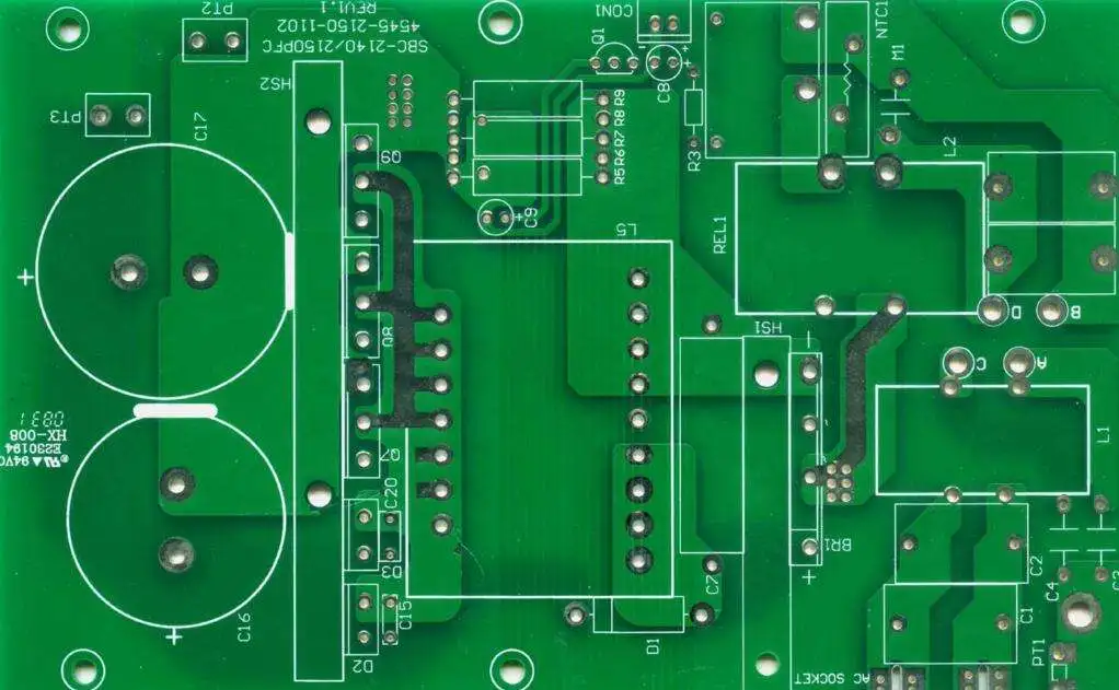
PCB silkscreen is the layer of ink or markings on a circuit board that provides text, symbols, or logos. These markings are crucial for identifying components, indicating polarity, or adding assembly instructions. While silkscreen is commonly applied to the top layer of a PCB, adding it to the bottom layer can be just as useful, especially for double-sided boards where components are mounted on both sides.
For hobbyists, a bottom layer silkscreen can help during soldering, troubleshooting, or even showcasing your design. It adds a polished, professional appearance to your homemade PCB silkscreen projects. In the following sections, we'll dive into the tools, materials, and methods you need to achieve this at home, focusing on techniques like toner transfer silkscreen for cost-effective results.
Tools and Materials for DIY PCB Silkscreen on the Bottom Layer
Before starting, gather the necessary tools and materials. Most of these are affordable and easy to find, making this a beginner-friendly process for hobbyist PCB manufacturing.
- Copper-Clad Board: A double-sided board for etching circuits on both layers.
- Laser Printer: Essential for printing your silkscreen design using the toner transfer method.
- Glossy Photo Paper or Toner Transfer Paper: Used to transfer the design to the PCB. Glossy paper works well for sharp, clean transfers.
- Household Iron: For transferring the toner from the paper to the PCB surface.
- Acetone or Nail Polish Remover: To clean the board and remove excess toner after transfer.
- Ferric Chloride or Etchant Solution: For etching the copper layers not covered by toner (if you're also etching the circuit).
- Protective Gear: Gloves and safety glasses to handle chemicals safely.
- Fine Sandpaper or Steel Wool: To clean the copper surface before transferring the design.
- Design Software: Free tools like open-source PCB design software to create your silkscreen layout.
With these tools in hand, you're ready to start the process of applying a homemade PCB silkscreen to the bottom layer.
Step-by-Step Guide to Applying Silkscreen to the Bottom Layer
Let’s break down the process of creating a DIY PCB silkscreen for the bottom layer. This method focuses on the toner transfer silkscreen technique, which is ideal for hobbyists due to its simplicity and low cost.
Step 1: Design Your Silkscreen Layout
Start by creating your silkscreen design using PCB design software. Focus on the bottom layer, ensuring that text, symbols, or logos are clear and legible. Remember to mirror the design for the bottom layer since you'll be transferring it directly onto the board. Keep lines and text at least 0.8mm thick to ensure they transfer properly without smudging.
Print the design using a laser printer on glossy photo paper or specialized toner transfer paper. The toner acts as a mask that will transfer to the PCB surface, so ensure the print is dark and sharp.
Step 2: Prepare the PCB Surface
Clean the bottom side of your double-sided copper-clad board thoroughly. Use fine sandpaper or steel wool to remove oxidation and create a smooth surface for the toner to adhere to. After sanding, wipe the board with acetone or rubbing alcohol to remove any dust or grease. A clean surface is critical for a successful toner transfer silkscreen.
Step 3: Transfer the Toner to the Bottom Layer
Place the printed design face down on the bottom side of the PCB, aligning it carefully. Secure it with heat-resistant tape if needed to prevent shifting. Preheat a household iron to a medium-high setting (around 150-180°C or 300-350°F, depending on the iron). Gently press the iron over the paper for 2-3 minutes, applying even pressure to ensure the toner bonds with the copper surface.
Let the board cool for a few minutes, then carefully peel off the paper. If some toner didn’t transfer properly, you can touch it up with a permanent marker. Soak the board in warm water for 5-10 minutes to remove any remaining paper residue, then scrub gently with a soft brush.
Step 4: Protect the Silkscreen During Etching (If Needed)
If you’re also etching the bottom layer for circuitry, the silkscreen toner needs protection during the etching process. Ferric chloride or other etchants can damage unprotected toner. To avoid this, apply a thin layer of clear nail polish or a UV-curable mask over the silkscreen areas after the toner has fully adhered. This step is optional if you’ve already etched the board or if the bottom layer is only for silkscreen.
For etching, submerge the board in ferric chloride solution for 10-20 minutes, agitating occasionally. Check the progress to avoid over-etching. Once done, rinse the board with water and remove the protective layer (if applied) using acetone.
Step 5: Finalize and Inspect the Silkscreen
After transferring the toner (and etching, if applicable), inspect the silkscreen on the bottom layer. If some areas are faint, use a fine-tip permanent marker to reinforce the markings. For a more durable finish, apply a clear coat of spray lacquer or conformal coating over the silkscreen to protect it from wear during soldering or handling.
Tips for Success with Homemade PCB Silkscreen
Creating a DIY PCB silkscreen for the bottom layer can be tricky at first, but these tips will help improve your results and streamline the process for hobbyist PCB manufacturing.
- Test Your Printer Settings: Adjust the printer to the highest toner density for darker, more reliable transfers. Experiment with a scrap piece of paper to confirm the settings.
- Use Even Heat Distribution: When ironing, move the iron slowly and evenly to avoid hotspots that can smear the toner.
- Double-Check Alignment: Ensure the silkscreen design aligns with any existing circuitry or holes on the bottom layer. Misalignment can make the markings useless.
- Work in a Well-Ventilated Area: If using chemicals like acetone or ferric chloride for PCB etching on the bottom layer, ensure proper ventilation to avoid inhaling fumes.
- Practice on Scrap Boards: If you’re new to toner transfer silkscreen, practice the process on a small piece of copper-clad board before working on your final project.
Common Challenges and How to Overcome Them
Even with careful preparation, you might run into issues during the DIY PCB silkscreen process. Here are some common problems and solutions tailored for hobbyists.
Issue 1: Toner Doesn’t Transfer Fully
If parts of the design fail to transfer, it could be due to insufficient heat, uneven pressure, or a dirty PCB surface. Re-clean the board, increase the ironing time by 30-60 seconds, and ensure even pressure across the design. Using fresh toner transfer paper can also help.
Issue 2: Silkscreen Smudges or Blurs
Smudging often happens due to excessive heat or moving the paper during ironing. Lower the iron temperature slightly (try 140-160°C or 280-320°F) and secure the paper tightly with tape before starting. If smudging still occurs, touch up the design with a fine-tip marker.
Issue 3: Silkscreen Fades During Etching
If you’re etching the bottom layer, the toner may erode in the etchant solution. Protect the silkscreen with a layer of clear nail polish or a UV mask before etching. Alternatively, apply the silkscreen after etching to avoid exposure to chemicals.
Why Choose Toner Transfer for DIY PCB Silkscreen?
The toner transfer silkscreen method stands out as a go-to technique for hobbyists due to its simplicity and affordability. Unlike professional silkscreen printing, which requires specialized equipment and inks, toner transfer uses everyday items like a laser printer and household iron. It’s perfect for small-scale projects and allows you to experiment with custom designs without breaking the bank.
Additionally, toner transfer works well for both single-sided and double-sided boards, making it versatile for various hobbyist PCB manufacturing needs. While it may not achieve the precision of industrial methods, it offers a practical solution for labeling and personalizing your homemade PCBs.
Enhancing Your PCB with Color Silkscreen (Optional)
If you want to take your DIY PCB silkscreen to the next level, consider adding color to the bottom layer markings. While traditional toner transfer results in black markings, you can use colored permanent markers or specialized toner foils (available online) to add vibrant accents after the transfer process. Apply the color carefully to avoid covering critical circuit areas, and seal it with a clear coat for durability.
Colored silkscreen is purely aesthetic but can make your board stand out, especially if you’re showcasing your work or creating a unique design for a project.
Conclusion: Mastering DIY PCB Silkscreen for the Bottom Layer
Applying a silkscreen to the bottom layer of your PCB at home is a rewarding way to elevate your hobbyist PCB manufacturing projects. With the toner transfer silkscreen method, you can achieve professional-looking results using simple tools and materials. From designing your layout to transferring the toner and protecting the markings, each step is manageable with patience and practice.
By following this guide, you now have the know-how to tackle PCB etching for the bottom layer and add clear, useful silkscreen markings. Whether you’re labeling components or adding a personal touch to your homemade PCB silkscreen, this process opens up new possibilities for creativity and functionality in your designs. Start small, experiment with different techniques, and watch your skills grow with each board you create.


