 ALLPCB


In the fast-evolving world of electronics, power supply printed circuit boards (PCBs) play a vital role in ensuring devices operate efficiently and reliably. If you're searching for insights on power supply PCB trends, power supply PCB innovations, power supply PCB technology, or next-gen power supply PCB solutions, you're in the right place. This blog dives deep into the future of power supply PCBs, exploring cutting-edge advancements and emerging trends that are shaping the industry. From miniaturization to sustainability, we'll cover the technologies driving the next generation of power supply designs and how they impact engineers and manufacturers.
Why Power Supply PCBs Are Critical to Modern Electronics
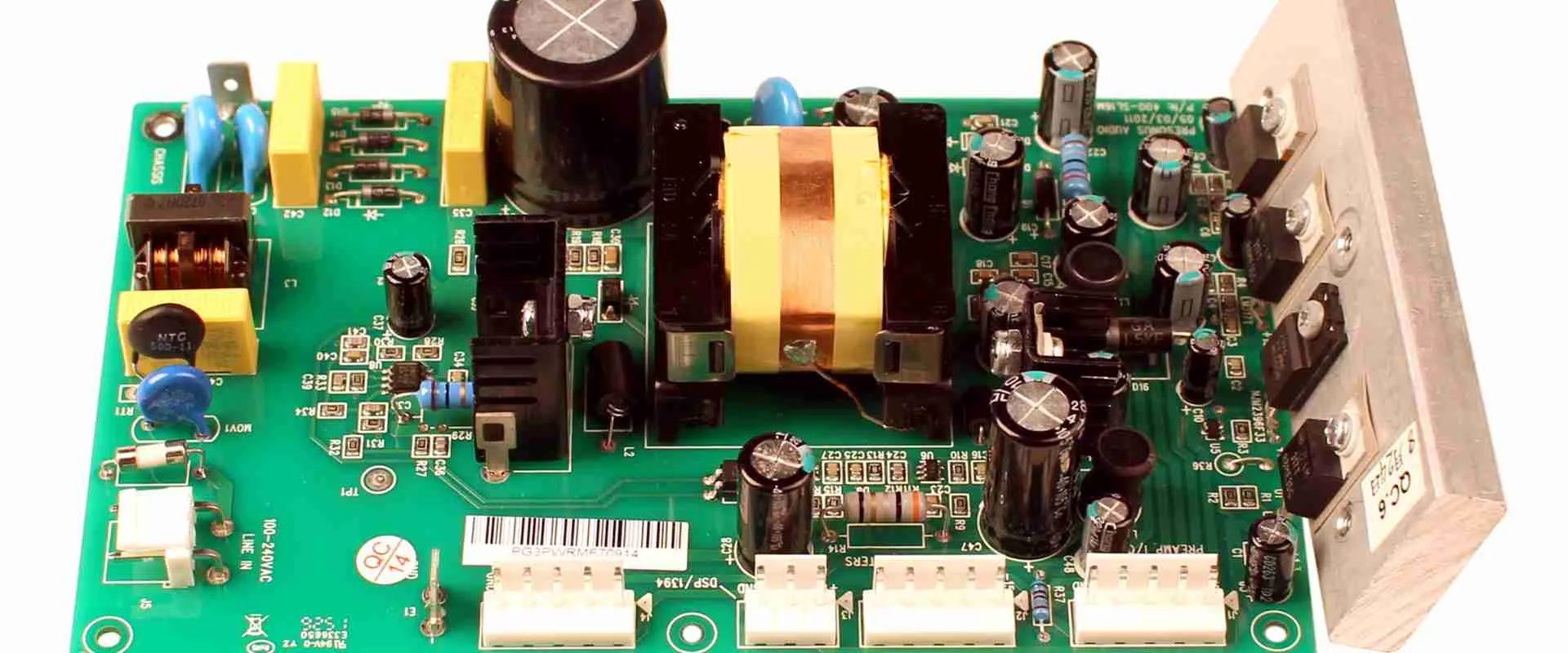
Power supply PCBs are the backbone of any electronic device, converting and distributing electrical power to components with precision. Whether it's a smartphone, industrial machinery, or an electric vehicle, these boards ensure stable voltage and current, protecting sensitive components from damage. As devices become smaller, faster, and more energy-efficient, the demand for advanced power supply PCB technology grows. The future of these boards lies in addressing challenges like heat dissipation, energy efficiency, and compact design while meeting the needs of emerging applications.
Key Trends Shaping Power Supply PCB Development
The landscape of power supply PCBs is changing rapidly due to technological advancements and industry demands. Below are the major power supply PCB trends that are defining the future.
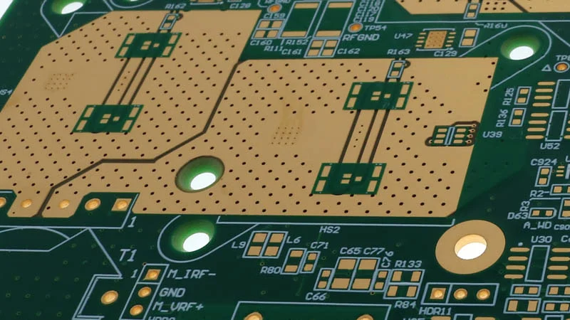
1. Miniaturization and High-Density Interconnect (HDI) Technology
As devices shrink in size, power supply PCBs must follow suit. Miniaturization is a driving force in power supply PCB innovations, with High-Density Interconnect (HDI) technology leading the charge. HDI PCBs use microvias and fine lines to pack more components into smaller spaces, often reducing board size by up to 30% compared to traditional designs. This allows for compact power supplies in applications like wearables and IoT devices, where space is at a premium.
For instance, microvias with diameters as small as 0.1 mm enable shorter signal paths, reducing impedance and improving power delivery efficiency. This is critical for high-speed devices where even a 1% loss in efficiency can lead to significant heat buildup. Engineers can now design power supply PCBs that support higher current densities while maintaining thermal stability.
2. Enhanced Thermal Management Solutions
Heat dissipation remains a top challenge in power supply PCB design, especially as power demands increase. Modern devices often operate at higher voltages and currents, generating heat that can degrade performance or damage components. Next-gen power supply PCB designs are incorporating advanced thermal management techniques to tackle this issue.
One popular solution is the use of thermal vias—small conductive pathways that transfer heat away from critical components to a heat sink or metal layer. Additionally, materials like ceramic-based substrates, which offer thermal conductivity up to 170 W/m·K compared to traditional FR4's 0.3 W/m·K, are gaining traction for high-power applications. These innovations ensure that power supply PCBs remain reliable even under heavy loads, extending the lifespan of electronic devices.
3. Adoption of Wide Bandgap Semiconductors
Wide bandgap (WBG) semiconductors, such as silicon carbide (SiC) and gallium nitride (GaN), are revolutionizing power supply PCB technology. These materials can handle higher voltages, temperatures, and switching frequencies compared to traditional silicon-based components. For example, GaN transistors can operate at switching frequencies above 1 MHz, compared to silicon's typical 100 kHz, enabling smaller and more efficient power supply designs.
The result is a significant reduction in energy loss—often by 20-40%—and a smaller footprint for components like inductors and capacitors. This trend is particularly impactful in electric vehicles and renewable energy systems, where efficiency directly affects performance and cost. Power supply PCBs integrating WBG semiconductors are setting new standards for energy efficiency in next-gen applications.
Innovations Driving Next-Gen Power Supply PCBs
Beyond trends, specific power supply PCB innovations are paving the way for groundbreaking designs. These advancements address both technical challenges and broader industry goals like sustainability and scalability.
1. Smart Power Management Integration
Smart power management is becoming a cornerstone of next-gen power supply PCB designs. By integrating microcontrollers and sensors directly onto the PCB, engineers can monitor and adjust power delivery in real-time. This is especially useful in applications like data centers, where power usage can fluctuate dramatically. Smart PCBs can reduce energy waste by up to 15% by dynamically adjusting voltage levels based on load requirements.
For example, a power supply PCB with embedded sensors can detect overheating and lower power output to prevent damage. This level of intelligence not only improves efficiency but also enhances the reliability of critical systems, making it a game-changer for industries reliant on uninterrupted power.
2. Sustainable Materials and Eco-Friendly Manufacturing
Sustainability is no longer just a buzzword; it's a priority in PCB manufacturing. The push for eco-friendly practices is influencing power supply PCB trends through the use of recyclable materials and lead-free soldering processes. Traditional PCB substrates like FR4 are being supplemented with biodegradable alternatives or materials with lower environmental impact.
Moreover, additive manufacturing techniques, such as 3D printing, are reducing material waste during production by up to 50%. These methods also allow for rapid prototyping of power supply PCBs, cutting down development time for engineers. As regulations around electronic waste tighten, adopting sustainable practices in PCB design will become essential for compliance and market competitiveness.
3. Modular and Scalable Designs
Modularity is an emerging innovation in power supply PCB technology, allowing engineers to create scalable power solutions for diverse applications. Modular PCBs consist of interchangeable sections that can be customized or upgraded without redesigning the entire board. This approach reduces costs and speeds up production, as manufacturers can reuse core designs across multiple products.
For instance, a modular power supply PCB for industrial equipment might include a base layer for core power distribution and optional modules for specific voltage or current requirements. This flexibility is ideal for industries like telecommunications, where power needs vary widely between projects. Scalable designs also make it easier to integrate future upgrades, ensuring that power supply PCBs remain relevant as technology evolves.
Applications of Next-Gen Power Supply PCBs
The advancements in power supply PCB innovations are unlocking new possibilities across various sectors. Here’s how these technologies are being applied in real-world scenarios.
1. Electric Vehicles (EVs) and Renewable Energy
Electric vehicles and renewable energy systems are among the biggest beneficiaries of modern power supply PCBs. EVs require compact, high-efficiency power supplies to manage battery charging and power distribution. With WBG semiconductors and advanced thermal management, power supply PCBs in EVs can achieve efficiencies above 95%, reducing energy loss and extending driving range.
Similarly, renewable energy systems like solar inverters rely on efficient power supply PCBs to convert and store energy with minimal loss. As the world shifts toward greener technologies, the role of advanced PCBs in these applications will only grow.
2. Consumer Electronics and IoT Devices
From smartphones to smart home devices, consumer electronics are pushing the boundaries of miniaturization and efficiency. Next-gen power supply PCB designs using HDI technology allow manufacturers to create slimmer devices without sacrificing performance. For IoT devices, low-power designs and smart power management ensure longer battery life, often extending operation by days or weeks on a single charge.
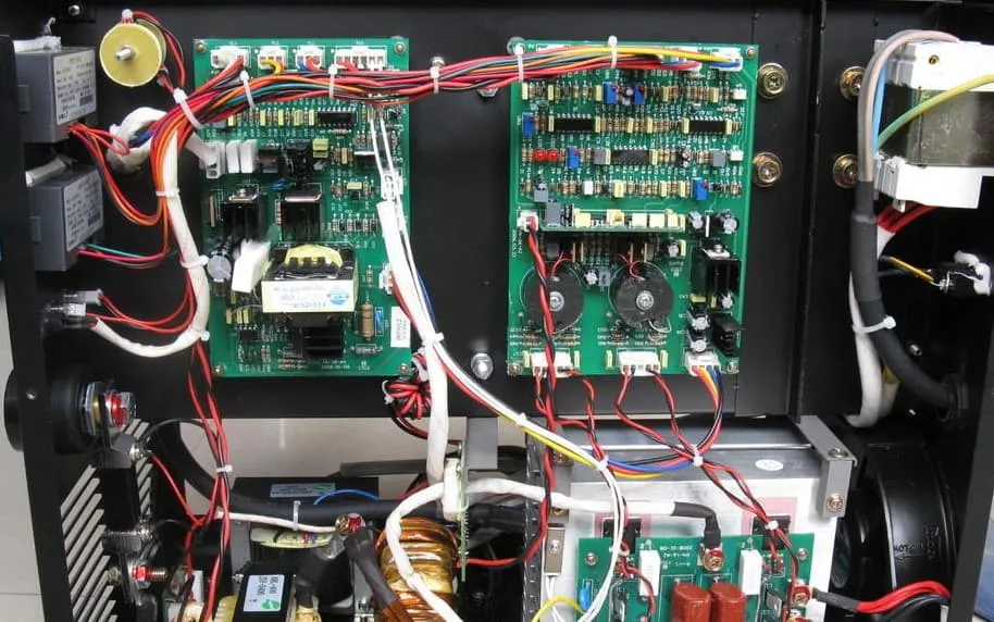
3. Industrial and Medical Equipment
In industrial and medical settings, reliability is paramount. Power supply PCBs with smart monitoring and robust thermal management ensure that critical equipment operates without interruption. For example, medical devices like MRI machines require stable power delivery with minimal noise interference, which modern PCB designs can achieve through optimized layouts and advanced materials.
Challenges in Adopting New Power Supply PCB Technologies
While the future of power supply PCBs is bright, there are hurdles to overcome. The adoption of advanced materials and technologies often comes with higher costs, which can be a barrier for smaller manufacturers. Additionally, designing PCBs for high-frequency applications or extreme environments requires specialized expertise and tools, adding complexity to the development process.
However, as manufacturing techniques improve and economies of scale kick in, these challenges are expected to diminish. Collaboration between engineers, material scientists, and manufacturers will be key to making power supply PCB innovations more accessible and affordable.
How to Stay Ahead with Power Supply PCB Trends
For engineers and businesses, staying updated with power supply PCB trends is essential to remain competitive. Start by exploring the latest materials and design techniques that align with your project needs. Partnering with a trusted PCB manufacturing service can also provide access to cutting-edge technologies and expertise, ensuring your designs are future-proof.
Investing in simulation and testing tools can help optimize power supply PCB layouts for efficiency and reliability before production. Finally, keep an eye on industry developments, as new standards and regulations may influence design requirements in the coming years.
Conclusion: The Road Ahead for Power Supply PCBs
The future of power supply PCBs is defined by innovation, efficiency, and adaptability. From miniaturization with HDI technology to sustainable manufacturing and smart power management, power supply PCB technology is evolving to meet the demands of a connected, energy-conscious world. These power supply PCB trends and power supply PCB innovations are not just shaping the electronics of tomorrow—they’re enabling breakthroughs in industries ranging from automotive to healthcare.
As we move forward, embracing next-gen power supply PCB solutions will be crucial for engineers and manufacturers aiming to create reliable, high-performance devices. By understanding and leveraging these advancements, you can design power supply PCBs that power the future with efficiency and precision.


