ALLPCB


Minimum trace spacing plays a critical role in determining PCB impedance, which directly impacts signal integrity in high-speed electronic designs. When traces are placed too close together or spaced improperly, it can lead to impedance mismatches, crosstalk, and signal degradation. In this comprehensive guide, we’ll explore how trace spacing influences characteristic impedance and controlled impedance, and provide practical tips to optimize your PCB layout for better performance.
Whether you’re designing a simple circuit board or a complex high-frequency system, understanding the relationship between trace spacing, trace width, and PCB impedance is essential. Let’s dive into the details of how these factors interact and why they matter for signal integrity.
What Is PCB Impedance and Why Does It Matter?
PCB impedance refers to the resistance a signal encounters as it travels along a trace on a printed circuit board. Specifically, characteristic impedance is the inherent impedance of a transmission line, determined by the physical properties of the trace and the surrounding materials. Controlled impedance, on the other hand, is the deliberate design of traces to maintain a specific impedance value, often required in high-speed circuits to prevent signal reflections and distortions.
Impedance matters because mismatches can cause signal integrity issues, such as reflections, delays, and data loss. For high-speed designs operating at frequencies above 100 MHz, even small variations in impedance can degrade performance. This is where trace spacing and width come into play, as they directly affect the impedance of a PCB trace.
The Role of Minimum Trace Spacing in PCB Design
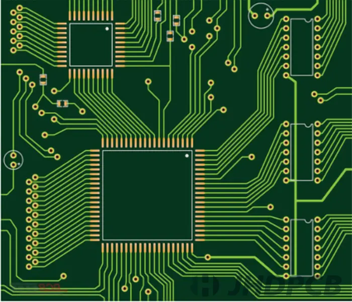
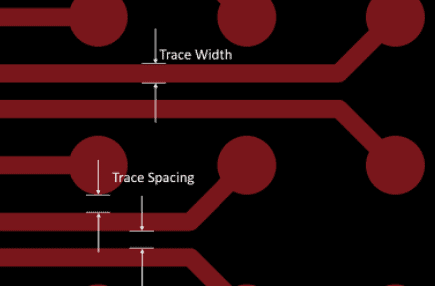
Minimum trace spacing refers to the smallest allowable distance between two adjacent traces on a PCB. This spacing is determined by manufacturing constraints, electrical requirements, and design standards. While it might seem like a minor detail, trace spacing has a significant impact on PCB impedance and overall signal integrity.
When traces are too close together, electromagnetic fields from one trace can interfere with another, leading to crosstalk—a phenomenon where signals unintentionally couple between traces. This interference alters the effective impedance of the traces, making it harder to maintain controlled impedance. Additionally, improper spacing can increase parasitic capacitance between traces, further affecting signal performance.
How Trace Spacing Affects Characteristic Impedance
Characteristic impedance (often denoted as Z?) is calculated based on several factors, including trace width, trace thickness, dielectric constant of the PCB material, and the distance between the trace and its reference plane (usually a ground plane). While trace spacing isn’t directly part of the characteristic impedance formula for a single trace, it becomes crucial when dealing with differential pairs or multiple traces in close proximity.
For a single microstrip trace (a trace on the outer layer of a PCB with a ground plane beneath), the characteristic impedance can be approximated using the following formula:
Z? = (87 / √(εr + 1.41)) * ln(5.98h / (0.8w + t))
Where:
- εr is the dielectric constant of the PCB material (e.g., 4.5 for FR4).
- h is the height of the dielectric between the trace and the ground plane (e.g., 0.2 mm).
- w is the width of the trace (e.g., 0.15 mm).
- t is the thickness of the trace (e.g., 0.035 mm).
While this formula doesn’t include trace spacing, the proximity of adjacent traces introduces mutual capacitance and inductance, which can alter the effective impedance. For instance, if two traces are spaced only 0.1 mm apart, the parasitic capacitance between them could reduce the effective impedance by 5-10%, depending on the frequency and material properties.
In differential pair routing, trace spacing is even more critical. Differential pairs rely on tightly controlled impedance (often 100 ohms for USB or Ethernet signals) to ensure that the two traces carry complementary signals without interference. If the spacing between the pair is inconsistent or too close to other traces, the differential impedance can deviate, leading to signal mismatch and data errors.
Trace Width and Spacing: A Balancing Act for Controlled Impedance
Controlled impedance design requires careful balancing of trace width and spacing. Wider traces generally have lower impedance, while narrower traces have higher impedance. However, adjusting trace width to achieve a target impedance (e.g., 50 ohms for many RF applications) often necessitates changes in spacing as well.
For example, if you’re designing a PCB with a target impedance of 50 ohms using a standard FR4 material (dielectric constant of 4.5), a trace width of approximately 0.3 mm and a dielectric height of 0.2 mm might be ideal for a microstrip configuration. However, if adjacent traces are spaced less than 0.3 mm apart, the mutual capacitance could lower the effective impedance to 45 ohms or less, causing signal reflections.
To mitigate this, designers often increase trace spacing to at least 3 times the trace width (a common rule of thumb) to minimize crosstalk and maintain controlled impedance. For high-speed signals above 1 GHz, even larger spacing—up to 5 times the trace width—may be necessary.

Signal Integrity Challenges Caused by Improper Trace Spacing
Signal integrity refers to the quality of an electrical signal as it travels through a PCB. Poor trace spacing can introduce several signal integrity issues, including:
- Crosstalk: As mentioned earlier, closely spaced traces can couple signals, leading to noise and interference. For high-speed signals, crosstalk can cause bit errors and reduce data reliability.
- Impedance Mismatch: Variations in trace spacing can lead to inconsistent impedance along a transmission line, causing signal reflections. Reflections can distort waveforms and degrade performance, especially in systems operating at 500 MHz or higher.
- Signal Delay: Parasitic capacitance from closely spaced traces can slow down signal propagation, introducing unwanted delays. This is particularly problematic in timing-critical applications like DDR memory interfaces.
To illustrate, consider a high-speed USB 3.0 design requiring a differential impedance of 90 ohms. If the traces in the differential pair are spaced too closely (e.g., 0.1 mm instead of the recommended 0.2 mm), the increased capacitance could lower the impedance to 80 ohms. This mismatch might result in a signal reflection loss of up to 10%, significantly impacting data transfer rates.
Practical Tips for Optimizing Trace Spacing in PCB Design
Designing a PCB with optimal trace spacing to maintain controlled impedance and signal integrity doesn’t have to be daunting. Here are some actionable tips to guide you through the process:
- Follow Design Rules: Adhere to minimum spacing guidelines provided by your PCB manufacturer. For standard designs, a spacing of at least 0.15 mm is often sufficient, but high-speed designs may require 0.3 mm or more.
- Use Impedance Calculators: Leverage online tools or software to calculate the required trace width and spacing for your target impedance. Many tools account for dielectric properties and layer stackup to provide accurate results.
- Maintain Consistent Spacing: Ensure uniform spacing between traces, especially in differential pairs. Inconsistent spacing can introduce impedance variations along the signal path.
- Incorporate Ground Planes: Place ground planes near signal traces to reduce electromagnetic interference and stabilize impedance. A solid ground plane can act as a shield, minimizing the impact of trace spacing on crosstalk.
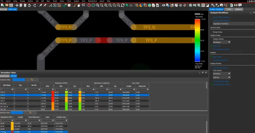
- Test and Simulate: Use simulation software to model your PCB layout and identify potential signal integrity issues before manufacturing. Simulations can reveal how trace spacing affects impedance at different frequencies.
The Impact of PCB Materials on Trace Spacing and Impedance
Beyond trace spacing and width, the choice of PCB material also influences impedance. The dielectric constant (εr) of the substrate material affects how electromagnetic fields propagate around traces. For instance, FR4, a common PCB material, has a dielectric constant of approximately 4.5, while high-frequency materials like Rogers 4350B have a lower value of around 3.5.
A lower dielectric constant allows for wider trace spacing without significantly altering impedance, as the electromagnetic fields are less confined. However, high-frequency materials are often more expensive, so designers must balance cost and performance. When working with standard materials like FR4, tighter control over trace spacing becomes even more critical to achieve the desired characteristic impedance.
Common Standards for Trace Spacing and Impedance Control
Several industry standards guide trace spacing and impedance control in PCB design. Familiarizing yourself with these can help ensure compliance and optimal performance:
- IPC-2221: This standard provides guidelines for PCB design, including minimum trace spacing based on voltage and environmental conditions. For example, at 50V, a minimum spacing of 0.13 mm is recommended for internal layers.
- IPC-2141: Focused on controlled impedance, this standard offers detailed formulas and recommendations for designing transmission lines with specific impedance values.
- USB and Ethernet Standards: High-speed protocols often specify exact impedance requirements (e.g., 90 ohms for USB differential pairs) and suggest trace spacing to achieve these values.
By aligning your design with these standards, you can minimize signal integrity issues and ensure compatibility with industry expectations.
Conclusion: Mastering Trace Spacing for Better PCB Impedance
Minimum trace spacing is a fundamental aspect of PCB design that directly affects impedance and signal integrity. By understanding how spacing interacts with trace width, dielectric materials, and layout configurations, you can design boards that maintain controlled impedance and deliver reliable performance, even at high frequencies.
From adhering to design rules and using simulation tools to selecting the right materials, every step in the design process contributes to achieving optimal PCB impedance. As electronic devices continue to push the boundaries of speed and complexity, mastering trace spacing will remain a cornerstone of successful PCB design.
Take the time to carefully plan your trace layouts and consider the impact of spacing on characteristic impedance. With the right approach, you can avoid common pitfalls like crosstalk and signal reflections, ensuring your designs meet the demands of modern electronics.