 ALLPCB


If you're diving into the world of printed circuit boards (PCBs), you've likely come across the term "PCB silkscreen." But what exactly is it, and why does it matter? PCB silkscreen is a layer of non-conductive ink applied to a circuit board to display text, symbols, and markings. These markings help identify components, test points, and other critical information, making assembly and troubleshooting much easier. In this comprehensive guide, we'll explore everything you need to know about PCB silkscreen techniques, materials, PCB silkscreen printing methods, and best practices to ensure your board designs are clear, functional, and professional.
Whether you're an engineer, designer, or hobbyist, understanding the ins and outs of PCB silkscreen can save you time, reduce errors, and improve the overall quality of your projects. Let’s break it down step by step with actionable insights and practical tips.
What Is PCB Silkscreen and Why Is It Important?
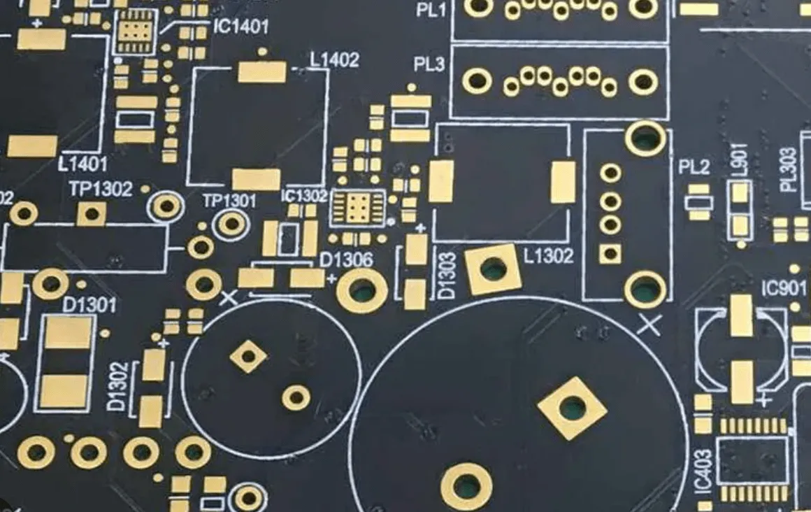
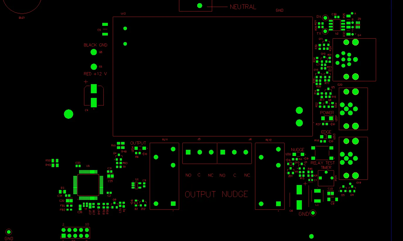
PCB silkscreen, often called "legend printing," is the process of applying ink to the surface of a printed circuit board to label components, indicate polarity, mark test points, and provide other useful information. Typically applied on the component side of the board, though sometimes on the solder side as well, this layer uses a non-conductive epoxy ink that won't interfere with the board's electrical functionality.
The importance of PCB silkscreen cannot be overstated. It acts as a visual guide during assembly, helping technicians place components correctly. For troubleshooting, it allows engineers to quickly identify parts without referring to schematics constantly. Additionally, silkscreen can include warnings, logos, or version numbers, adding a professional touch to the board. Without clear silkscreen markings, the risk of assembly errors or misinterpretations increases significantly, potentially leading to costly rework or failures.
PCB Silkscreen Techniques: Exploring the Options
When it comes to applying silkscreen on a PCB, there are several techniques available, each with its own advantages and limitations. Understanding these PCB silkscreen techniques can help you choose the right method for your project based on precision, cost, and production volume.
1. Manual Screen Printing
Manual screen printing is one of the oldest and most straightforward PCB silkscreen printing methods. It involves using a stencil or mesh screen to apply ink directly onto the PCB surface. A squeegee pushes the ink through the screen, transferring the design onto the board. This method is often used for low-volume production or prototypes due to its simplicity and low cost.
However, manual screen printing lacks precision for intricate designs or fine text. It’s also labor-intensive and not ideal for high-volume manufacturing, where consistency is critical. If you're working on a small batch of boards with basic markings, this technique can still be a viable option.
2. Liquid Photo Imaging (LPI)
Liquid Photo Imaging, or LPI, is a more advanced and widely used technique for PCB silkscreen. In this method, a photo-sensitive ink is applied to the PCB surface, and a photographic mask is used to expose specific areas to UV light. The unexposed areas are then washed away, leaving behind the desired markings. LPI offers high precision, making it suitable for detailed designs and small text, often down to 0.15 mm line width.
This technique is popular in medium to high-volume production because of its accuracy and repeatability. It’s also more durable than manual printing, as the ink bonds well with the board surface. However, the setup cost for LPI can be higher due to the need for specialized equipment and masks.
3. Direct Legend Printing (DLP)
Direct Legend Printing is a modern PCB silkscreen technique that uses inkjet printing technology to apply markings directly onto the PCB. This method eliminates the need for screens or masks, as a digital file controls the printer to deposit ink precisely where needed. DLP is highly flexible, allowing for quick design changes without additional setup costs.
DLP is ideal for prototypes or small runs where frequent design iterations are common. It can achieve fine details with line widths as small as 0.1 mm. However, the ink used in DLP may not be as durable as that in LPI, and the process can be slower for large-scale production.
PCB Silkscreen Materials: What You Need to Know
The materials used in PCB silkscreen play a crucial role in the durability, readability, and overall quality of the markings. Let’s dive into the common PCB silkscreen materials and their characteristics to help you make informed decisions for your projects.
1. Epoxy Ink
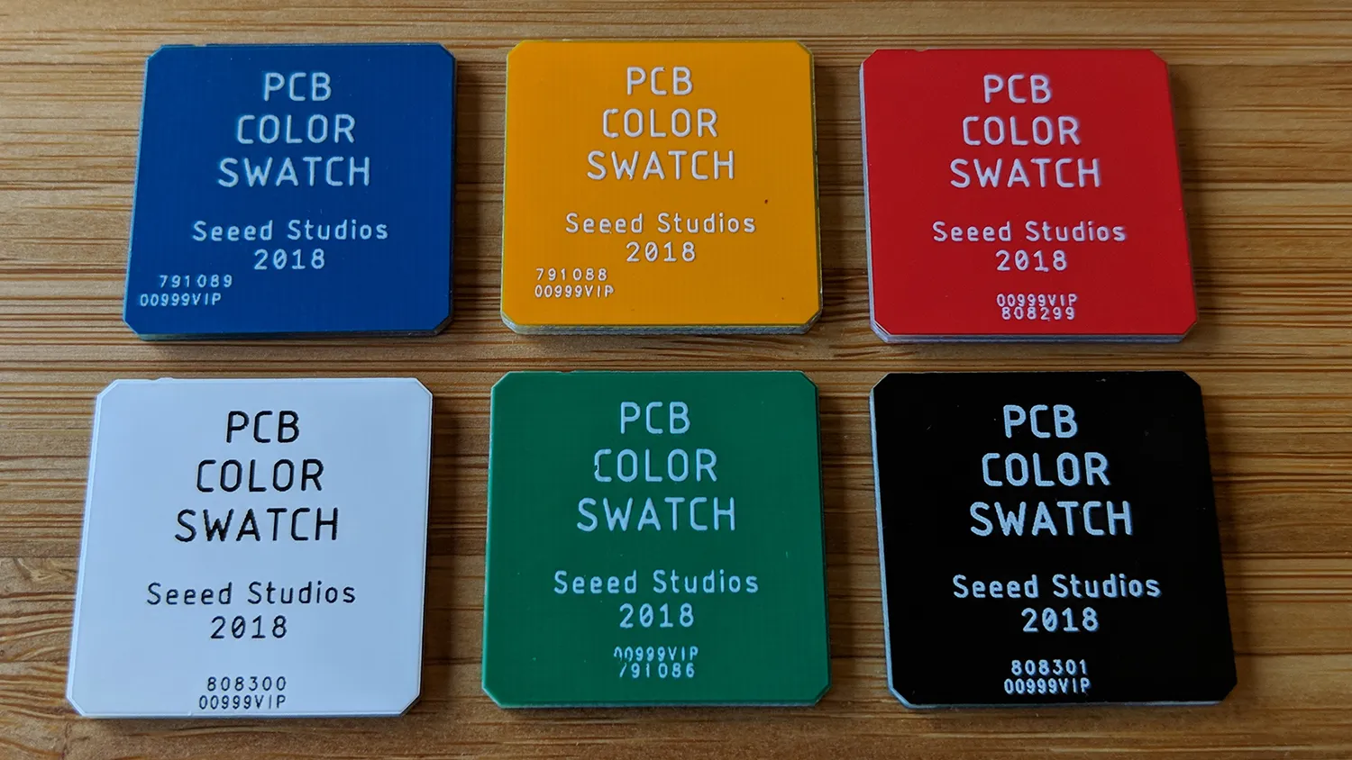
Epoxy ink is the most commonly used material for PCB silkscreen. This non-conductive ink is durable and resistant to chemicals, heat, and abrasion, making it ideal for harsh environments. Epoxy ink adheres well to the PCB surface and can withstand the soldering process without degrading. It’s available in standard colors like white, black, and yellow, with white being the most popular due to its high contrast on green solder masks.
2. Acrylic Ink
Acrylic ink is another option for PCB silkscreen, often used in less demanding applications. While it’s less expensive than epoxy ink, it doesn’t offer the same level of durability or resistance to environmental factors. Acrylic ink may fade or wear off over time, especially in high-temperature or chemically aggressive settings. It’s more suitable for prototypes or indoor applications where the PCB won’t face extreme conditions.
3. Color and Contrast Considerations
Choosing the right color for your silkscreen ink is essential for readability. White ink is the industry standard because it contrasts well with most solder mask colors, such as green or blue. Black ink can be used on lighter solder masks, while yellow is sometimes chosen for specific aesthetic or branding purposes. Ensure the ink color provides at least a 70% contrast ratio with the background for optimal visibility under standard lighting conditions.
PCB Silkscreen Best Practices for Optimal Results
Creating a high-quality silkscreen layer requires attention to detail and adherence to proven PCB silkscreen best practices. These guidelines will help you avoid common pitfalls and ensure your markings are clear, useful, and professional.
1. Keep Text and Symbols Clear and Legible
Always use a font size that’s readable, ideally no smaller than 6 points (about 0.8 mm in height). Avoid overly complex fonts with thin lines or intricate details, as they may not print clearly. Stick to standard sans-serif fonts like Arial or Helvetica for maximum clarity. For symbols, ensure they are universally recognized, such as polarity indicators or ground symbols, to prevent confusion during assembly.
2. Position Markings Strategically
Place silkscreen markings close to the components they refer to, but avoid overlapping with pads, vias, or other critical areas where solder or components might obscure the text. For densely populated boards, prioritize labeling only the most critical components to avoid clutter. If space is limited, consider using reference designators (e.g., R1 for resistor 1) rather than full descriptions.
3. Limit Silkscreen to One Side When Possible
While silkscreen can be applied to both the component and solder sides of a PCB, adding it to the solder side often increases manufacturing costs. Unless absolutely necessary, limit silkscreen to the component side to keep expenses down. If markings are needed on both sides, ensure they are aligned with the board’s design files to prevent errors during production.
4. Verify Design Files Before Production
Always double-check your silkscreen layer in your PCB design software before sending files to manufacturing. Ensure that text and symbols are correctly placed and not mirrored or misaligned. Many design tools allow you to preview the silkscreen layer in 3D, helping you spot potential issues like overlapping text or unclear markings.
5. Consider Environmental Factors
If your PCB will be exposed to harsh conditions, such as high humidity, extreme temperatures, or chemical exposure, choose a durable ink like epoxy and confirm with your manufacturer that the silkscreen process can withstand these factors. For example, boards used in automotive or industrial applications often require silkscreen that remains legible after exposure to temperatures up to 125°C.
PCB Silkscreen Printing Methods: Choosing the Right Process
Selecting the appropriate PCB silkscreen printing methods ties closely to the techniques discussed earlier. Here’s a deeper look at how these methods impact cost, quality, and production timelines, helping you align your choice with project needs.
Cost vs. Quality Trade-Offs
Manual screen printing is the most cost-effective for small runs, often costing as little as $0.10 per board for basic designs in low quantities. However, the quality may vary, with potential misalignments or uneven ink application. LPI offers better quality at a higher cost, typically around $0.50 per board for medium volumes, due to the need for masks and equipment setup. DLP, while expensive at approximately $1.00 per board for prototypes, provides unmatched flexibility for design changes without additional setup fees.
Production Speed and Scalability
For high-volume production, LPI is often the fastest method, as it can be integrated into automated manufacturing lines, processing hundreds of boards per hour. Manual printing, on the other hand, is slow and labor-intensive, suitable only for batches of fewer than 50 boards. DLP sits in the middle, offering quick turnaround for small runs (under 100 boards) but slowing down as quantities increase due to the inkjet process.
Common Challenges in PCB Silkscreen and How to Avoid Them
Even with the best techniques and materials, issues can arise during PCB silkscreen application. Here are some common challenges and tips to overcome them.
1. Ink Smearing or Fading
Ink smearing often occurs due to improper curing or handling during manufacturing. To avoid this, ensure the ink is fully cured using the recommended temperature (typically 150°C for 30 minutes for epoxy ink) before further processing. Fading can result from using low-quality ink or exposing the board to harsh conditions beyond its limits. Opt for high-quality materials and test your boards under expected operating conditions.
2. Misalignment of Markings
Misaligned silkscreen can make a board look unprofessional and confuse assemblers. This issue often stems from errors in design files or manufacturing setup. Always provide clear, high-resolution design files and confirm with your manufacturer that they’ve aligned the silkscreen layer correctly before production begins.
3. Overcrowded Silkscreen
Too many markings can clutter the board, making it hard to read. Focus on essential information only, such as component designators and polarity indicators. For complex boards, consider including a separate assembly drawing or documentation instead of overloading the silkscreen layer.
Conclusion: Mastering PCB Silkscreen for Better Designs
PCB silkscreen is a small but critical part of printed circuit board design and manufacturing. By understanding the various PCB silkscreen techniques like manual printing, LPI, and DLP, selecting the right PCB silkscreen materials such as epoxy or acrylic ink, and following PCB silkscreen best practices, you can create boards that are easier to assemble, troubleshoot, and maintain. Whether you're working on a prototype or a high-volume production run, paying attention to silkscreen details can elevate the quality and professionalism of your projects.
Armed with the insights from this guide, you’re ready to tackle your next PCB design with confidence. Focus on clarity, durability, and strategic placement of markings, and always collaborate closely with your manufacturing partner to ensure the silkscreen layer meets your expectations. With these steps, your PCBs will not only function flawlessly but also look polished and professional.


