 ALLPCB


Designing a gaming console PCB layout is a complex yet rewarding process that bridges the gap between a conceptual schematic and a fully functional device. Whether you're a hobbyist or a professional engineer searching for a "gaming console PCB layout tutorial," this guide will walk you through each step with clarity and precision. We'll explore tools like Altium Designer and Eagle for creating a gaming console PCB, along with tips for PCB routing and choosing the right design software. Let's dive into the detailed process of bringing your gaming console from an idea to a working circuit board.
Why Gaming Console PCB Layout Matters
The printed circuit board (PCB) is the heart of any gaming console, connecting components like processors, graphics chips, memory modules, and power systems. A well-designed PCB layout ensures high performance, minimal signal interference, and efficient heat dissipation—crucial for a device that runs intensive games for hours. Poor layout design can lead to issues like lag, overheating, or even hardware failure. This guide will help you master the "gaming console PCB layout tutorial" process, ensuring your design is optimized for performance and reliability.
Step 1: Understanding the Basics of Gaming Console PCB Design
Before diving into software tools or routing techniques, it's essential to grasp the unique requirements of a gaming console PCB. These devices often handle high-speed signals (up to 5 GHz for modern graphics processing), require multiple power domains (e.g., 1.2V for CPU, 3.3V for I/O), and need robust thermal management. Your layout must account for signal integrity, electromagnetic interference (EMI), and component density.
Start by defining your design goals. Are you creating a compact handheld console or a high-performance desktop system? This decision impacts board size, layer count (often 6-12 layers for complex consoles), and component selection. Once you have a clear vision, you can move to the schematic phase.
Step 2: Creating a Schematic for Your Gaming Console
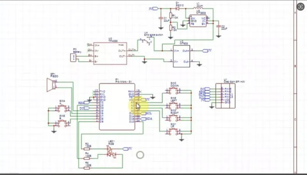
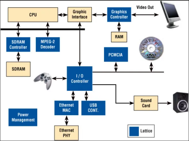
The schematic is the blueprint of your PCB, showing how components are electrically connected. For a gaming console, you'll need to include key elements like a central processing unit (CPU), graphics processing unit (GPU), RAM, storage controllers, input/output ports (HDMI, USB), and power management circuits.
Use design software to draw your schematic. Two popular options for "gaming console PCB design software" are widely-used tools that cater to both beginners and professionals. These tools allow you to create detailed schematics with libraries of components tailored for high-speed designs. When placing components in the schematic, group them by function (e.g., power supply, processing, connectivity) to simplify the layout phase.
Ensure that high-speed signals, like those between the CPU and GPU, are prioritized for direct connections to minimize latency. For example, DDR memory signals often require matched trace lengths with tolerances as tight as ±10 mils to prevent timing issues. Double-check your schematic for errors before proceeding to the layout stage.
Step 3: Choosing the Right Software for Gaming Console PCB Design
Selecting the appropriate "gaming console PCB design software" can make or break your project. Two powerful options stand out for their capabilities in handling complex designs like gaming consoles.
Option 1: Altium Designer for Gaming PCB
Altium Designer is a top-tier tool for "Altium Designer gaming PCB" projects due to its advanced features. It supports multi-layer designs, high-speed signal routing, and 3D visualization, which are essential for gaming consoles. With built-in simulation tools, you can test signal integrity and power distribution before manufacturing. Its interface allows for seamless transition from schematic to layout, making it ideal for complex projects with tight deadlines.
Option 2: Eagle for Gaming Console PCB
Eagle is another excellent choice for "Eagle PCB gaming console" designs, especially for hobbyists or small teams. It offers a user-friendly interface and extensive component libraries, though it may lack some of the advanced simulation features of other high-end tools. Eagle is perfect for simpler console designs or prototypes, allowing you to focus on layout and routing without a steep learning curve.
Both tools support exporting Gerber files, the universal format for PCB manufacturing, ensuring compatibility with fabrication processes. Choose based on your project complexity and budget, as licensing costs can vary significantly.
Step 4: Transitioning from Schematic to PCB Layout
Once your schematic is complete, import it into the PCB editor of your chosen software. This step involves placing components on the board and routing connections between them. For a gaming console, component placement is critical due to space constraints and performance needs.
Begin by placing high-priority components like the CPU and GPU in central locations to minimize trace lengths for high-speed signals. Position power management ICs near these components to reduce voltage drops, ideally maintaining a drop of less than 5% (e.g., from 1.2V to 1.14V). Place decoupling capacitors (typically 0.1 μF to 1 μF) close to power pins to filter noise.
Next, define your board stackup. A typical gaming console PCB might use an 8-layer stackup, with dedicated layers for power, ground, and signal routing. Ground planes are essential for reducing EMI and providing a stable reference for high-speed signals. Ensure impedance control for critical traces, targeting values like 50 ohms for single-ended signals or 100 ohms for differential pairs.
Step 5: Mastering PCB Routing for Gaming Consoles
Routing is where the "PCB routing gaming console" challenge truly comes into play. This step involves creating physical connections (traces) between components while adhering to design rules for signal integrity and manufacturability.
High-Speed Signal Routing
Gaming consoles rely on high-speed signals for data transfer between CPU, GPU, and memory. Route these signals on inner layers with adjacent ground planes to minimize interference. Maintain consistent trace widths (e.g., 5-8 mils for high-speed lines) and avoid sharp corners, using 45-degree angles or curves to prevent signal reflection.
Power and Ground Distribution
Create solid power and ground planes to ensure stable voltage delivery. Split power planes if your design uses multiple voltages (e.g., 1.8V for memory, 3.3V for I/O), but avoid routing high-speed signals over splits to prevent noise. Use vias strategically to connect components to power and ground layers, keeping via inductance low by using multiple small vias (e.g., 10 mil diameter) instead of one large via.
Thermal Management
Gaming consoles generate significant heat, especially from processors. Place thermal vias under high-power components to transfer heat to a copper layer or heatsink. Ensure traces near these areas are not too thin, as heat can cause resistance to increase, potentially leading to failures.
Step 6: Design Rule Checks and Validation
Before finalizing your layout, run design rule checks (DRC) in your software to identify errors like overlapping traces, unconnected nets, or clearance violations. For gaming consoles, set strict clearance rules (e.g., 6 mils between traces) to prevent short circuits. Check impedance matching for high-speed signals and ensure power delivery networks can handle current demands (e.g., 2-5A for GPU).
Use simulation tools if available to analyze signal integrity and thermal performance. For instance, simulate crosstalk on adjacent traces, aiming for levels below -40 dB to avoid interference. Address any issues by adjusting trace spacing or adding shielding.
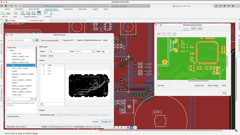
Step 7: Generating Manufacturing Files
Once your layout passes all checks, generate the necessary files for manufacturing. These include Gerber files for each layer (copper, silkscreen, solder mask) and a drill file for vias. Include a bill of materials (BOM) listing all components with their specifications. Double-check that your files match the manufacturer's requirements, such as minimum trace widths (often 4-6 mils) and via sizes.
Consider adding a silkscreen layer with labels for key components and connectors. This makes assembly and troubleshooting easier, especially for complex gaming console designs.
Step 8: Prototyping and Testing
After manufacturing, assemble a prototype of your gaming console PCB. Test for functionality, focusing on power stability, signal timing, and thermal performance. Use an oscilloscope to measure signal rise times (ideally under 1 ns for high-speed lines) and check for voltage ripple on power lines (aim for less than 50 mV). If issues arise, revisit your layout to adjust routing or component placement.
Tips for Optimizing Your Gaming Console PCB Layout
- Minimize Layer Transitions: Keep high-speed signals on a single layer when possible to avoid via-induced delays.
- Use Differential Pairs: For signals like USB or HDMI, route as differential pairs with matched lengths to maintain timing.
- Prioritize Cooling: Integrate heat sinks or thermal pads early in the design to manage temperatures during long gaming sessions.
- Iterate Designs: Build multiple prototypes to refine your layout based on real-world performance data.
Conclusion: Bringing Your Gaming Console to Life
Designing a gaming console PCB layout is a meticulous process that requires attention to detail, from schematic creation to final routing. By following this "gaming console PCB layout tutorial," using tools tailored for "Altium Designer gaming PCB" or "Eagle PCB gaming console" projects, and mastering "PCB routing gaming console" techniques, you can create a high-performance board ready for the market. With the right "gaming console PCB design software" and a structured approach, your journey from schematic to screen will be a success.
Partner with a reliable fabrication service to bring your design to reality. At ALLPCB, we’re committed to supporting engineers with high-quality manufacturing solutions tailored to complex projects like gaming consoles. Start your design today and turn your vision into a playable device!


