In the world of modern electronics, achieving signal integrity in high-density PCBs with BGA (Ball Grid Array) components is a critical challenge. As devices become smaller and more powerful, the need for precise design techniques to manage signal integrity on BGA PCBs grows. This blog post dives deep into the essentials of BGA breakout strategies and high-density PCB design to ensure your signals remain clear and reliable, even in the most compact layouts. Whether you're an engineer tackling complex designs or a designer looking to optimize performance, this guide offers practical insights and actionable tips.
What Is BGA Breakout and Why Does Signal Integrity Matter?
BGA breakout refers to the process of routing signals from the densely packed pins of a Ball Grid Array component to other parts of a printed circuit board (PCB). Due to the high pin count and tight spacing of BGA packages, maintaining signal integrity—ensuring that signals travel without distortion, noise, or interference—becomes a significant hurdle in high-density PCB designs. Poor signal integrity can lead to data errors, reduced performance, or complete system failure, especially in high-speed applications like telecommunications, computing, and automotive electronics.
In this comprehensive guide, we’ll explore the key challenges of BGA breakout, proven techniques to preserve signal integrity, and best practices for high-density PCB layouts. Let’s break it down step by step to help you design robust and efficient boards.
Understanding the Challenges of BGA Breakout in High-Density PCBs
Before diving into solutions, it’s important to understand the unique challenges that come with BGA components on high-density PCBs:
- High Pin Density: BGA packages can have hundreds or even thousands of pins in a small area, often with a pitch (spacing between pins) as tight as 0.4mm. Routing these signals without overlap or interference is a complex task.
- Signal Crosstalk: Close proximity of traces increases the risk of crosstalk, where signals interfere with each other, degrading performance.
- Impedance Mismatch: Inconsistent trace widths or improper layer stackups can cause impedance mismatches, leading to signal reflections and loss.
- Power Delivery Issues: High-density designs often struggle with providing stable power to BGA components, leading to noise in the power distribution network (PDN).
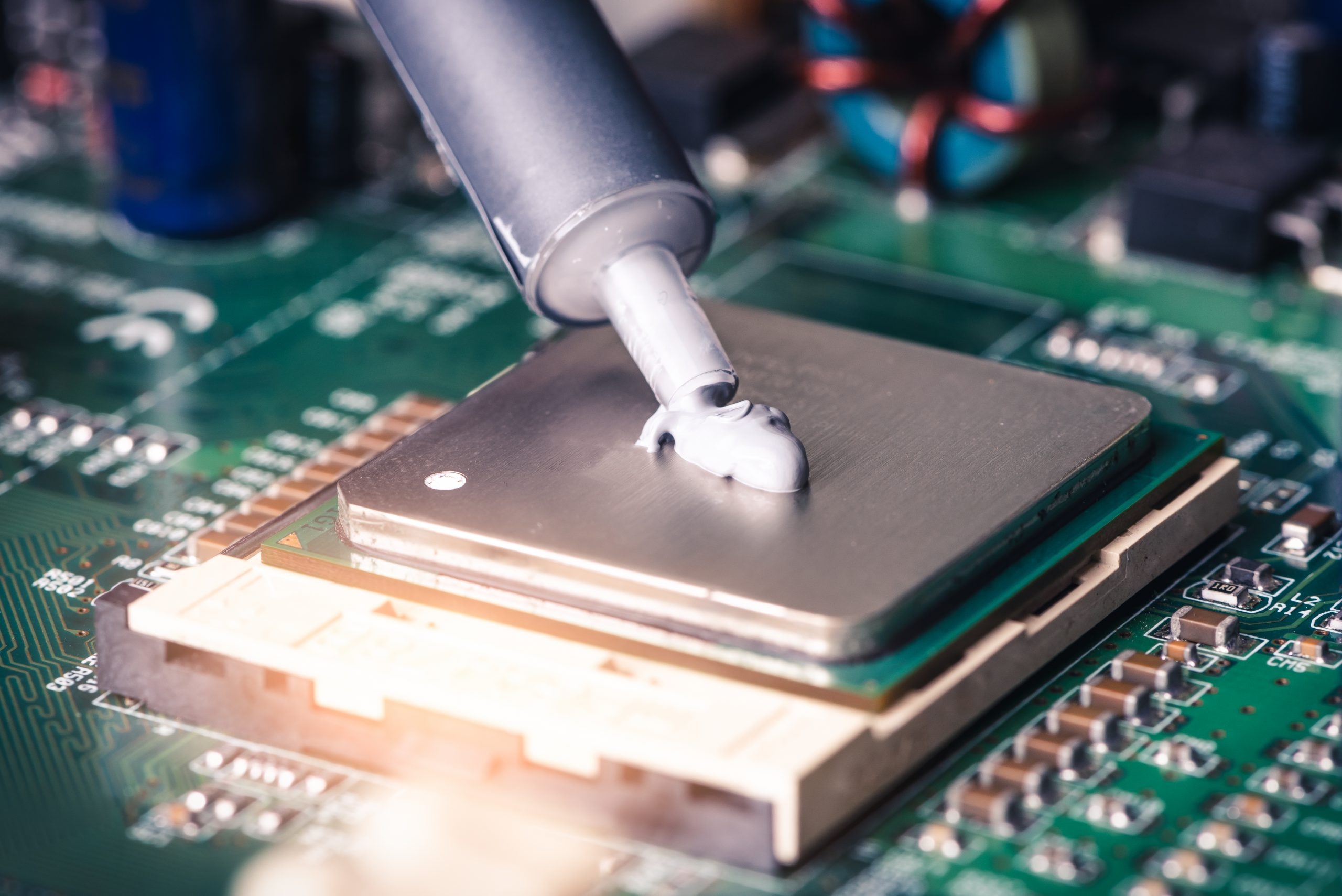
- Thermal Management: The compact nature of high-density PCBs can trap heat, impacting signal integrity and component reliability.
These challenges highlight the need for careful planning and precise design techniques to ensure signal integrity in BGA PCB layouts.
Key Techniques for BGA Breakout and Signal Integrity
Let’s explore proven strategies to achieve successful BGA breakout while maintaining signal integrity in high-density PCB designs. These methods focus on layout optimization, routing practices, and material selection.
1. Optimize Your BGA Fanout Strategy
BGA fanout is the process of routing signals from the inner pins of a BGA to the outer layers of the PCB for easier access. A well-planned fanout strategy is the foundation of signal integrity. Here are key tips:
- Use Dog-Bone Fanout: For larger BGA packages with a pitch of 0.8mm or more, a dog-bone fanout pattern (a short trace connecting the BGA pad to a via) works well. This allows signals to escape the dense grid efficiently.
- Via-in-Pad for Tight Pitches: For finer pitches (0.5mm or less), placing vias directly in the BGA pads can save space and reduce trace length, minimizing signal loss. Ensure proper manufacturing processes to avoid soldering issues.
- Staggered Vias: Stagger vias in a zigzag pattern to maximize spacing between traces and reduce crosstalk.
By carefully planning fanout, you can reduce congestion and ensure cleaner signal paths. For example, in a design with a 1mm pitch BGA having 256 pins, a dog-bone fanout can route signals to outer layers within two to three PCB layers, maintaining trace widths of 5 mils for controlled impedance.
2. Prioritize Controlled Impedance in Routing
Signal integrity heavily depends on maintaining consistent impedance along signal paths. Impedance mismatches can cause reflections, leading to signal distortion. Here’s how to manage it:
- Match Trace Widths and Spacing: Use trace width calculators to ensure traces meet the target impedance, often 50 ohms for single-ended signals or 100 ohms for differential pairs in high-speed designs.
- Route on Appropriate Layers: Place high-speed signals on inner layers sandwiched between ground planes to shield them from external noise and maintain impedance.
- Avoid Sharp Corners: Use 45-degree angles or rounded corners for trace bends to prevent signal reflection, especially for signals operating at frequencies above 1 GHz.
For instance, a high-speed signal running at 2.5 GHz on a standard FR-4 material PCB requires a trace width of approximately 6 mils and a spacing of 12 mils from adjacent traces to achieve a 50-ohm impedance, assuming a 4-layer stackup with a dielectric constant of 4.2.
3. Minimize Crosstalk with Proper Spacing and Shielding
Crosstalk occurs when signals interfere with each other due to close proximity. In high-density PCB designs, where space is limited, reducing crosstalk is critical:
- Maintain Adequate Spacing: Follow the 3W rule—keep spacing between parallel traces at least three times the trace width to minimize coupling. For a 5-mil trace, aim for 15 mils of separation.
- Use Ground Planes: Place continuous ground planes adjacent to signal layers to act as a shield and provide a return path for signals, reducing electromagnetic interference (EMI).
- Route Differential Pairs Together: For high-speed differential signals, route pairs closely with consistent spacing to ensure balanced signal propagation and cancel out noise.
These practices can significantly lower crosstalk, ensuring cleaner signals in your BGA PCB design.
4. Design a Robust Power Distribution Network (PDN)
A stable power supply is essential for signal integrity, especially in high-density designs with BGA components that demand high current. Noise in the PDN can directly impact signal quality. Consider these tips:
- Use Decoupling Capacitors: Place low-ESR (Equivalent Series Resistance) capacitors near BGA power pins to filter out high-frequency noise. For a BGA with a 1.2V core voltage, use a mix of 0.1μF and 1μF capacitors within 100 mils of the pins.
- Optimize Power Planes: Dedicate entire layers to power and ground in your stackup to minimize impedance and ensure even current distribution.
- Minimize Via Inductance: Use multiple vias for power connections to reduce inductance, which can cause voltage drops. For high-current BGA pins, aim for at least two to three vias per pin.
A well-designed PDN ensures that your BGA component receives clean power, directly benefiting signal integrity.
5. Choose the Right Materials for High-Speed Signals
The choice of PCB material impacts signal integrity, especially for high-frequency applications common in BGA designs. Standard FR-4 material may not suffice for signals above 5 GHz due to higher dielectric loss.
- Low-Dk Materials: Use materials with a low dielectric constant (Dk) like Rogers or Isola for high-speed designs to reduce signal delay and loss. For example, Rogers 4350B with a Dk of 3.48 is ideal for signals up to 10 GHz.
- Low-Loss Tangent: Select materials with a low dissipation factor (Df) to minimize signal attenuation. A Df below 0.005 is recommended for high-frequency BGA PCBs.
Investing in high-performance materials can make a significant difference in maintaining signal integrity in high-density PCB layouts.
Best Practices for High-Density PCB Layout with BGA Components
Beyond specific techniques, adopting general best practices for high-density PCB design can further enhance signal integrity and manufacturability. Here are some key guidelines:
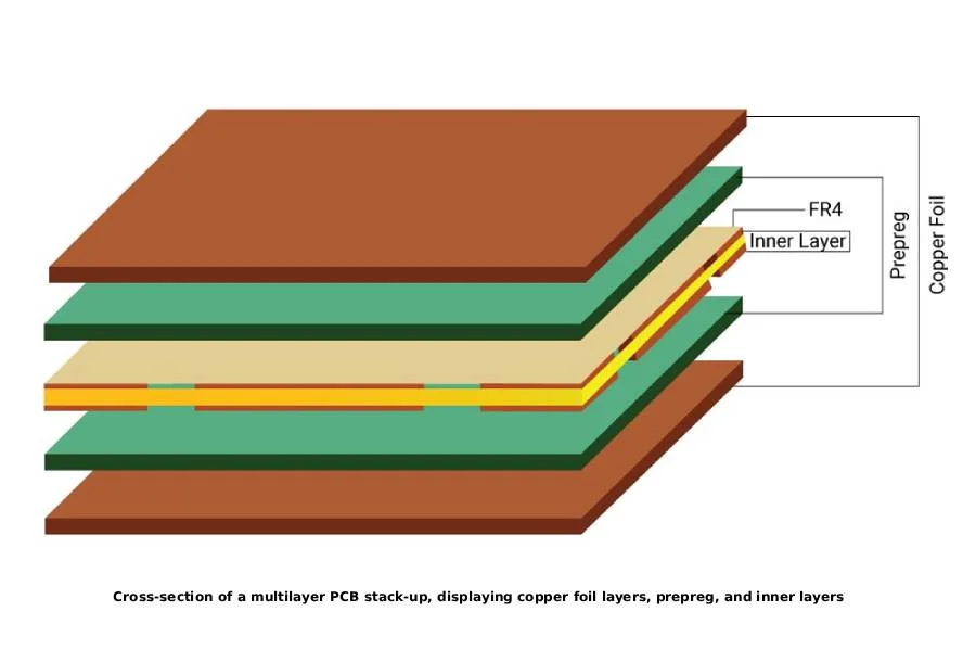
- Plan Your Stackup Early: Design a multilayer stackup (e.g., 6 to 12 layers) with dedicated signal, ground, and power layers. A typical 8-layer stackup might include two signal layers on top and bottom, with inner layers for ground and power.
- Simulate Before Fabrication: Use signal integrity simulation tools to model crosstalk, impedance, and power delivery before manufacturing. This can catch issues like signal reflections early in the design phase.
- Follow Design for Manufacturability (DFM) Rules: Ensure trace widths, via sizes, and clearances meet your fabricator’s capabilities to avoid production errors that could affect signal integrity.
- Keep High-Speed Signals Short: Minimize the length of critical signal traces to reduce propagation delay and loss. For a 5 GHz signal, aim to keep trace lengths under 2 inches on standard materials.
These practices create a solid foundation for successful BGA breakout and signal integrity in high-density PCB designs.
Common Pitfalls to Avoid in BGA PCB Design
Even with the best techniques, certain mistakes can compromise signal integrity. Watch out for these common pitfalls:
- Ignoring Ground Plane Continuity: Breaks or slots in ground planes can disrupt return paths, increasing noise and EMI.
- Overloading Layers: Trying to route too many signals on a single layer can lead to congestion and crosstalk. Use additional layers if needed.
- Neglecting Thermal Vias: Without proper thermal management, heat buildup under BGA components can degrade performance. Add thermal vias to dissipate heat to ground planes.
- Inconsistent Via Placement: Random or poorly placed vias can increase inductance and signal delay. Plan via locations strategically during fanout.
Avoiding these errors will save time and ensure your high-density PCB performs as intended.
Conclusion: Mastering Signal Integrity in BGA High-Density PCBs
Achieving signal integrity in high-density PCBs with BGA components requires a combination of careful planning, precise routing, and strategic material selection. By optimizing BGA breakout with techniques like dog-bone fanout or via-in-pad, maintaining controlled impedance, minimizing crosstalk, and designing a robust power distribution network, you can ensure reliable performance even in the most compact designs. Additionally, adhering to best practices and avoiding common pitfalls will further enhance your PCB’s success.
At ALLPCB, we’re committed to supporting engineers and designers in creating cutting-edge electronics with high-quality manufacturing solutions. Whether you’re working on a complex BGA PCB or a high-density design, these strategies will help you achieve signal integrity and build reliable, high-performance products.
 ALLPCB


