ALLPCB


In the fast-paced world of electronics, high-frequency PCB applications are at the heart of cutting-edge technologies like 5G, IoT, and advanced computing. For engineers designing these systems, maintaining signal integrity is a top priority. So, why is controlled depth drilling essential for high-frequency PCB applications? Simply put, controlled depth drilling, often referred to as back drilling, removes unused portions of vias in multilayer PCBs to minimize signal interference, reduce reflections, and ensure impedance matching for GHz signals. This technique is critical for achieving optimal performance in high-speed designs.
In this blog, we’ll dive deep into the importance of controlled depth drilling, explore its advantages, and explain how it supports high-frequency PCB drilling needs. Whether you’re working on telecommunications equipment or high-speed digital circuits, understanding this process can elevate your designs to the next level.
What Is Controlled Depth Drilling in PCB Manufacturing?
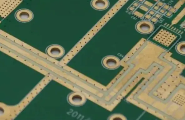
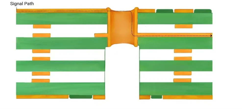
Controlled depth drilling, commonly known as back drilling, is a precision manufacturing technique used in the production of multilayer PCBs. It involves drilling through specific layers of a PCB to remove the unused stub of a via—a small conductive pathway that connects different layers of the board. These stubs, if left intact, can act as antennas, causing signal reflections and degrading performance, especially in high-frequency applications operating in the GHz range.
The process requires advanced machinery and precise control to drill only to a specified depth without damaging the functional parts of the via. By eliminating these stubs, back drilling ensures that signals travel along the intended path without interference, making it a go-to solution for high-speed and high-frequency PCB designs.
Why High-Frequency PCB Applications Demand Precision Drilling
High-frequency PCB applications, such as those used in 5G networks, radar systems, and high-speed data transfer, operate at frequencies often exceeding 1 GHz. At these frequencies, even tiny imperfections in the PCB can lead to significant signal loss, crosstalk, or reflections. Traditional through-hole vias, which span the entire thickness of the board, often leave unused stub sections that disrupt signal integrity.
For example, a via stub in a 10-layer PCB operating at 10 GHz can introduce a resonance that distorts the signal, leading to data errors or reduced system performance. Controlled depth drilling addresses this by removing the stub, ensuring the signal path is as clean and direct as possible. This precision is not just a luxury—it’s a necessity for maintaining the performance of high-frequency systems.
Key Advantages of Controlled Depth Drilling for High-Frequency PCBs
Controlled depth drilling offers several benefits that make it indispensable for high-frequency PCB designs. Let’s break down the most critical advantages, focusing on how they address common challenges like impedance matching and signal reflection reduction.
1. Improved Signal Integrity for GHz Signals
Signal integrity is the cornerstone of any high-frequency design. At GHz frequencies, signals are incredibly sensitive to disruptions caused by via stubs. These stubs can cause signal reflections, where part of the signal bounces back instead of traveling forward, leading to data corruption. Back drilling removes these stubs, minimizing reflections and ensuring the signal reaches its destination with minimal distortion.
For instance, in a PCB handling 5 GHz signals, removing via stubs through controlled depth drilling can reduce signal reflection by up to 50%, depending on the design and materials used. This results in clearer, more reliable data transmission, which is critical for applications like high-speed networking.
2. Enhanced PCB Impedance Matching
Impedance matching is vital in high-frequency designs to ensure that the signal travels through the PCB without loss or distortion. A mismatch in impedance—often caused by via stubs—can lead to signal reflections and energy loss. Controlled depth drilling helps maintain consistent impedance by eliminating the unused via portions that disrupt the electrical characteristics of the signal path.
In practical terms, achieving impedance values within a tight tolerance (e.g., ±10% of 50 ohms, a common standard for high-frequency signals) becomes far more feasible with back drilling. This precision ensures that your PCB performs reliably under demanding conditions.
3. Reduction in Electromagnetic Interference (EMI)
High-frequency signals are prone to generating and picking up electromagnetic interference (EMI), which can degrade performance and cause crosstalk between adjacent traces. Via stubs act as unintended radiators, amplifying EMI issues. By removing these stubs through controlled depth drilling, the potential for EMI is significantly reduced, leading to cleaner signal transmission and better overall system reliability.
4. Support for Higher Data Rates
As data rates continue to climb—think 10 Gbps and beyond for modern applications—PCBs must handle faster signal transitions without errors. Controlled depth drilling supports these high data rates by minimizing signal degradation. For example, in a multilayer PCB designed for 25 Gbps data transfer, back drilling can be the difference between meeting performance specs and facing costly redesigns due to signal loss.
How Controlled Depth Drilling Works in Practice
The process of controlled depth drilling is both an art and a science, requiring advanced equipment and skilled technicians. Here’s a step-by-step look at how it’s done:
- Design Analysis: Engineers identify which vias in the PCB layout have unused stubs that could affect signal integrity, particularly those involved in high-frequency signal paths.
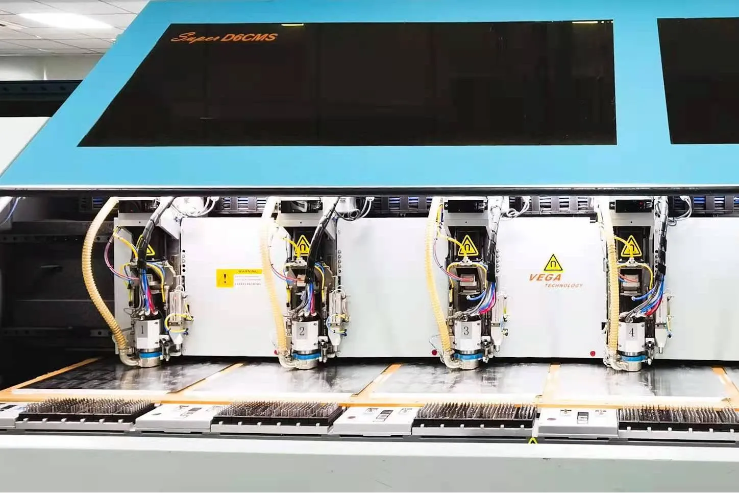
- Drilling Setup: Specialized CNC drilling machines are programmed to target specific vias, drilling from the back side of the PCB to a precise depth without affecting the functional layers.
- Depth Control: Advanced sensors and software ensure the drill stops at the exact depth, typically within a tolerance of ±0.05 mm, to avoid damaging the active via section.
- Inspection: Post-drilling inspection, often using X-ray or automated optical systems, verifies that the stubs are removed without compromising the PCB structure.
This meticulous process ensures that the final PCB meets the strict requirements of high-frequency applications, delivering reliable performance even under extreme conditions.
Applications of Controlled Depth Drilling in High-Frequency Designs
Controlled depth drilling is used across a wide range of industries where high-frequency and high-speed performance are critical. Some key applications include:
- Telecommunications: For 5G infrastructure and base stations, where signal integrity at GHz frequencies is non-negotiable.
- Data Centers: High-speed servers and networking equipment rely on back drilling to handle massive data throughput without errors.
- Aerospace and Defense: Radar and communication systems operating at high frequencies use this technique to ensure precision and reliability.
- Automotive: Advanced driver-assistance systems (ADAS) and vehicle-to-everything (V2X) communication systems benefit from improved signal quality.
In each of these fields, controlled depth drilling plays a pivotal role in meeting the stringent performance standards required for modern electronics.
Challenges and Considerations in Back Drilling for GHz Signals
While controlled depth drilling offers significant benefits, it’s not without challenges. Understanding these can help engineers make informed decisions during the design and manufacturing process.
1. Manufacturing Complexity
Back drilling requires highly specialized equipment and expertise, which can increase production costs and lead times. The process must be carefully planned to avoid errors, as a single misaligned drill can render a PCB unusable.
2. Design Constraints
Not all PCB designs are suitable for controlled depth drilling. For instance, densely packed boards with limited space between vias may pose challenges for precise drilling. Engineers must balance the benefits of back drilling with the practical limitations of their design.
3. Material Considerations
The choice of PCB material impacts the effectiveness of controlled depth drilling. High-frequency laminates, often used for GHz applications, can be more brittle or have different drilling characteristics compared to standard FR-4 materials, requiring tailored drilling parameters.
Despite these challenges, the advantages of controlled depth drilling far outweigh the drawbacks for most high-frequency applications, making it a worthwhile investment.
Tips for Optimizing High-Frequency PCB Drilling
To maximize the benefits of controlled depth drilling in your high-frequency PCB projects, consider the following tips during the design and manufacturing stages:
- Collaborate Early: Work closely with your manufacturing partner during the design phase to identify vias that require back drilling and ensure the layout supports the process.
- Use Simulation Tools: Employ signal integrity simulation software to predict the impact of via stubs on performance and determine where controlled depth drilling will have the most significant effect.
- Specify Tolerances: Clearly define depth tolerances and inspection criteria in your design files to avoid miscommunication during manufacturing.
- Choose the Right Materials: Select PCB materials optimized for high-frequency performance and compatible with precision drilling techniques.
By following these guidelines, you can ensure that your high-frequency PCB designs achieve the best possible results with controlled depth drilling.
Conclusion: The Future of High-Frequency PCB Design with Controlled Depth Drilling
As the demand for faster, more reliable electronics continues to grow, controlled depth drilling will remain a cornerstone of high-frequency PCB manufacturing. This technique addresses critical challenges like signal reflection reduction, PCB impedance matching, and overall signal integrity, making it essential for applications operating at GHz frequencies.
Whether you’re designing for 5G networks, high-speed data centers, or cutting-edge aerospace systems, back drilling offers a proven solution to enhance performance and reliability. By understanding its advantages and incorporating it into your design process, you can stay ahead in the ever-evolving world of electronics.
At ALLPCB, we’re committed to providing the precision manufacturing techniques you need to bring your high-frequency PCB designs to life. With expertise in controlled depth drilling and a focus on quality, we’re here to support your most ambitious projects.