If you're wondering about via-in-pad current carrying capacity, here's the quick answer: Via-in-pad designs can handle significant current, often up to 1-2 amps per via, depending on the via size, copper thickness, and thermal management. Factors like trace width, thermal resistance, and PCB power requirements play a big role in determining the exact capacity. In this detailed guide, we'll break down everything you need to know about vias in high-current PCB designs, including how to optimize for power and heat dissipation.
Introduction to Via-in-Pad Technology in PCB Design
In modern printed circuit board (PCB) design, via-in-pad technology has become a go-to solution for space-constrained layouts, especially in high-density interconnect (HDI) boards. Unlike traditional vias that are placed outside component pads, via-in-pad places the via directly under a component’s pad, saving valuable board space and improving signal integrity. But when it comes to high-current applications, a key concern arises: how much current can these vias carry without overheating or failing?
This blog dives deep into the concept of via current carrying capacity, exploring the relationship between trace width, thermal resistance, and PCB power needs. Whether you're an engineer working on high-current PCB designs or a hobbyist looking to understand the nuances of power routing, this guide will equip you with practical insights and actionable tips.
What Is Via-in-Pad and Why Does It Matter for Current Capacity?
Via-in-pad refers to a via (a vertical interconnect access) that is placed directly within the pad of a surface-mount component, such as a BGA (Ball Grid Array) or QFN (Quad Flat No-Lead) package. This design reduces the need for additional routing space, allowing for tighter layouts. However, when dealing with high-current PCB designs, the via must be capable of carrying the required current without excessive heat buildup or voltage drop.
The current carrying capacity of a via-in-pad depends on several factors, including the via diameter, the thickness of the copper plating inside the via (often 1 oz or 2 oz per square foot), and the surrounding thermal management strategies. A typical via with a 0.3 mm diameter and 1 oz copper plating might handle around 1.5 amps under normal conditions, but this can vary based on design specifics.
Understanding via current capacity is critical because overloading a via can lead to overheating, delamination of the PCB layers, or even complete failure of the circuit. In the following sections, we'll explore how to calculate and optimize this capacity for your designs.
Factors Affecting Via Current Carrying Capacity
Several elements influence how much current a via-in-pad can safely carry. Let’s break them down one by one to give you a clear picture of what to consider in your high-current PCB projects.
1. Via Size and Copper Thickness
The diameter of the via and the thickness of the copper plating inside it are primary determinants of current capacity. A larger via diameter allows for more copper surface area, which can carry higher currents. For instance, a via with a 0.5 mm diameter can often handle up to 2 amps, while a smaller 0.2 mm via might be limited to 0.8 amps. Copper thickness also matters—thicker plating (e.g., 2 oz/ft2) can handle more current compared to standard 1 oz/ft2 plating.
2. Trace Width Connected to the Via
The trace width leading to and from the via plays a significant role in current distribution. If the trace is too narrow, it can create a bottleneck, limiting the current even if the via itself can handle more. As a rule of thumb, for every 1 amp of current, a trace width of 10-15 mils (0.25-0.38 mm) is recommended for 1 oz copper at room temperature. Wider traces reduce resistance and heat buildup, ensuring the via isn’t overstressed.
3. Thermal Resistance and Heat Dissipation
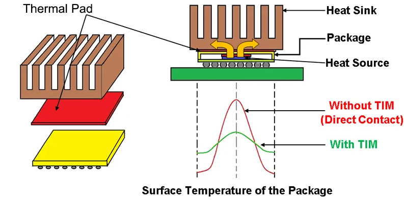
Thermal resistance is a measure of how much a via resists heat flow. High thermal resistance means heat gets trapped, raising the via’s temperature and potentially reducing its current carrying capacity. To combat this, designers often use thermal vias—additional vias placed near high-current areas to transfer heat to a ground plane or heat sink. For example, adding 4-6 thermal vias around a power component can reduce the temperature rise by 20-30°C.
4. PCB Power Requirements and Layer Stackup
The overall power requirements of your PCB also dictate via design. In high-current applications, such as power supplies or motor drivers, multiple vias may be needed in parallel to share the load. Additionally, the PCB layer stackup affects current distribution. A 4-layer board with dedicated power and ground planes can handle higher currents compared to a 2-layer board, as the planes provide low-resistance paths for current flow.
How to Calculate Via Current Carrying Capacity
Calculating the current carrying capacity of a via-in-pad isn’t just a guess—it’s a science. You can use specific formulas or online tools to get accurate values based on your design parameters. Here’s a step-by-step approach to doing it manually:
- Determine Via Dimensions: Measure the via diameter (e.g., 0.3 mm) and the copper thickness (e.g., 1 oz/ft2 or approximately 35 μm).
- Calculate Via Resistance: Use the formula R = ρ * L / A, where ρ is the resistivity of copper (1.68 x 10^-8 ohm-meters), L is the via length (board thickness, e.g., 1.6 mm), and A is the cross-sectional area of the copper plating (approximated as a cylinder wall). For a 0.3 mm via with 35 μm plating, the resistance might be around 0.5 milliohms.
- Estimate Power Loss: Power loss (P) is given by P = I2 * R, where I is the current. For 1 amp through a via with 0.5 milliohms resistance, the power loss is 0.0005 watts.
- Check Temperature Rise: Temperature rise depends on power loss and thermal resistance. A typical via might have a thermal resistance of 50°C/W, so a 0.0005 W loss results in a negligible 0.025°C rise. However, for higher currents, this rise can become significant.
For more accurate calculations, especially in complex designs, consider using online calculators tailored for PCB vias. These tools factor in additional variables like ambient temperature and board material (e.g., FR-4 with a thermal conductivity of 0.3 W/m·K).
Design Tips for Optimizing Via Current in High-Current PCBs
Designing for high-current PCB applications requires careful planning to ensure reliability and performance. Here are some practical tips to maximize via current carrying capacity while managing heat and power demands.
1. Use Multiple Vias for High Currents
If a single via can’t handle the required current, place multiple vias in parallel. For example, if your design needs to carry 5 amps and each via is rated for 1.5 amps, use at least 4 vias to distribute the load. This approach also helps with heat dissipation.
2. Increase Copper Thickness
Opt for thicker copper layers (e.g., 2 oz/ft2 or higher) in power-heavy designs. Thicker copper reduces resistance, allowing vias and traces to carry more current without overheating. Keep in mind that thicker copper may increase manufacturing costs, so balance this with your budget.
3. Incorporate Thermal Vias for Heat Management
Thermal vias are a must in high-power designs. Place them near components that generate significant heat, connecting them to ground or power planes to spread the heat across larger areas. A grid of 3x3 thermal vias under a power IC can drastically lower operating temperatures.
4. Optimize Trace Width for Current Flow
Match the trace width to the expected current. For instance, a 20-mil (0.5 mm) trace with 1 oz copper can safely carry about 2 amps without excessive heating. Wider traces also reduce voltage drops, ensuring stable power delivery to components.
5. Consider Via Filling for Enhanced Performance
In some high-current applications, filling vias with conductive materials (like copper or epoxy) can increase their current capacity and reduce thermal resistance. Filled vias are especially useful in via-in-pad designs for BGAs, as they provide a flat surface for soldering while improving electrical and thermal conductivity.
Common Challenges in High-Current Via Design and How to Overcome Them
Designing vias for high-current applications isn’t without its challenges. Here are some common issues and solutions to help you navigate them.
1. Overheating Due to Poor Thermal Management
Issue: High currents generate heat, and without proper dissipation, vias can overheat, leading to reliability issues.
Solution: Use thermal vias and connect them to large copper planes. Ensure adequate spacing between high-power components to prevent heat concentration.
2. Voltage Drops Across Narrow Traces
Issue: Narrow traces feeding into vias can cause significant voltage drops, affecting performance.
Solution: Widen traces to match current requirements and keep trace lengths short to minimize resistance.
3. Manufacturing Limitations for Small Vias
Issue: Very small vias in high-density designs may not support thick copper plating, limiting current capacity.
Solution: Work with your PCB manufacturer to balance via size and plating thickness. Consider slightly larger vias if current demands are high.
Conclusion: Mastering Via-in-Pad for High-Current PCB Designs
Via-in-pad technology offers incredible benefits for compact, high-density PCB designs, but its current carrying capacity must be carefully evaluated for high-power applications. By understanding the interplay between via size, trace width, thermal resistance, and PCB power needs, you can design reliable boards that handle significant currents without failure.
Start by calculating the expected via current using the methods outlined above, then apply design strategies like using multiple vias, increasing copper thickness, and adding thermal vias for heat management. With these practices, you'll ensure your high-current PCB designs are both efficient and durable, meeting the demands of even the most challenging projects.
Armed with this detailed guide, you're ready to tackle via-in-pad designs with confidence. Focus on optimizing every aspect of your layout, and your PCBs will deliver the performance and reliability your applications require.
 ALLPCB


