In high-frequency PCB design, vias play a critical role in connecting different layers of a circuit board. However, if not designed carefully, vias can introduce inductance and signal degradation, negatively impacting performance. So, how can you design vias to minimize these issues? The key lies in understanding via types, optimizing their placement, and following best practices for high-frequency applications. This blog post dives deep into via design strategies for high-frequency PCBs, focusing on minimizing inductance and ensuring signal integrity with actionable tips for engineers.
What Are PCB Vias and Why Do They Matter in High-Frequency Design?
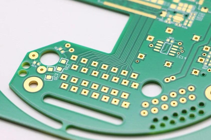
PCB vias are small conductive holes that create electrical connections between different layers of a printed circuit board. In high-frequency designs, where signals operate at gigahertz ranges, vias can act as unintended inductors or capacitors, disrupting signal integrity. Even a slight mismatch in impedance or excessive inductance can cause signal reflections, delays, or losses, leading to system failures.
For engineers working on high-speed applications like 5G, RF circuits, or high-speed digital systems, proper via design is non-negotiable. By optimizing via structures, you can maintain consistent impedance (often targeting 50 ohms for RF signals) and reduce parasitic effects that degrade performance.
Understanding Via Inductance in High-Frequency PCBs
Via inductance is a major concern in high-frequency PCB design. When a signal passes through a via, the structure acts like a small inductor due to its geometry and the current loop it creates. This inductance can cause signal delays or distortions, especially at frequencies above 1 GHz.
The inductance of a via depends on its length, diameter, and the surrounding dielectric material. A longer via, for instance, increases the inductive effect, while a smaller diameter can reduce it. As a rule of thumb, the inductance of a typical via is around 1-2 nH per millimeter of length. For a high-speed signal operating at 10 GHz, even a small inductance of 1 nH can introduce significant phase shifts or impedance mismatches.
To minimize via inductance, consider shorter vias and optimize their aspect ratio (the ratio of via length to diameter). Keeping the aspect ratio below 10:1 is often recommended for high-frequency designs to limit parasitic effects.
Types of PCB Vias for High-Frequency Applications
Not all vias are created equal. Choosing the right type of via can significantly impact signal integrity in high-frequency designs. Below are the main types of vias and their applications.
1. Through-Hole Vias
Through-hole vias extend through the entire thickness of the PCB, connecting the top and bottom layers. While they are simple to manufacture, they often have higher inductance due to their length, making them less ideal for high-frequency signals. If you must use through-hole vias, minimize their length by placing critical components on adjacent layers.
2. Blind Vias
Blind vias connect an outer layer to an inner layer without passing through the entire board. They are shorter than through-hole vias, reducing inductance and parasitic capacitance. Blind vias are ideal for high-frequency designs where signal paths need to be kept short, such as in multilayer boards for RF applications.
3. Buried Vias
Buried vias connect internal layers of the PCB without reaching the surface. Like blind vias, they offer lower inductance due to their reduced length. They are particularly useful in dense, multilayer designs where space is limited, and high-frequency signals need clean routing between internal layers.
Related Reading: What Are Vias—Choose The Via That Suits Your PCB Best
Via Stitching: Enhancing Signal Integrity and Reducing EMI
Via stitching involves placing multiple vias around a signal path or ground plane to create a low-impedance connection between layers. In high-frequency PCB design, via stitching is a powerful technique to reduce electromagnetic interference (EMI) and improve signal integrity.
For example, in RF designs, stitching vias are often placed around the edges of a ground plane to create a Faraday cage-like effect, minimizing noise coupling. A common guideline is to space stitching vias at a distance of λ/20 (where λ is the wavelength of the highest operating frequency). For a 5 GHz signal, with a wavelength of approximately 60 mm in air, this translates to a via spacing of about 3 mm.
Via stitching also helps in maintaining a consistent return path for high-frequency signals, reducing loop inductance. However, avoid overusing stitching vias, as excessive vias can increase manufacturing costs and potentially introduce unwanted resonances if not placed strategically.
Best Practices for High-Frequency Via Design
Designing vias for high-frequency PCBs requires careful planning. Below are some proven strategies to minimize inductance and signal degradation.
1. Keep Vias Short and Direct
The longer the via, the higher the inductance. Whenever possible, route high-frequency signals between adjacent layers to keep vias short. For instance, in a 10-layer PCB, routing a critical signal between layers 2 and 3 will result in less inductance compared to routing between layers 1 and 10.
2. Optimize Via Diameter and Pad Size
Smaller via diameters reduce inductance, but they must still be manufacturable. A via diameter of 0.2-0.3 mm is often a good balance for high-frequency designs. Additionally, minimize the size of via pads to reduce parasitic capacitance, which can also degrade signals. A pad diameter of 1.5 times the via diameter is a common starting point.
Related Reading: Decoding Minimum Drill Size for PCB Vias: A Signal Integrity Perspective
3. Use Back-Drilling for Through-Hole Vias
In high-frequency designs, through-hole vias often leave unused stubs that act as resonant structures, causing signal reflections. Back-drilling removes these stubs by drilling out the unused portion of the via after plating. This technique can reduce signal degradation significantly, especially for signals above 5 GHz.
4. Match Impedance with Via Design
Impedance mismatches at vias can cause signal reflections. To avoid this, design vias to maintain the characteristic impedance of the trace (typically 50 ohms for RF signals). This can be achieved by adjusting the via diameter, spacing, and surrounding ground planes. Simulation tools can help predict and optimize impedance during the design phase.
5. Place Ground Vias Strategically
Ground vias near signal vias provide a low-impedance return path, reducing loop inductance. Place ground vias within 1-2 mm of high-frequency signal vias to minimize noise and ensure a clean signal transition between layers.
Advanced Techniques for Minimizing Signal Degradation
Beyond basic via design, advanced techniques can further enhance performance in high-frequency PCBs.
1. Use Microvias for Dense Designs
Microvias are small-diameter vias (typically less than 0.15 mm) created using laser drilling. They are ideal for high-density interconnects (HDI) in multilayer boards, offering lower inductance and capacitance due to their small size. Microvias are especially useful in modern high-frequency applications like 5G modules or advanced microprocessors.
2. Implement Via-in-Pad Design
In via-in-pad design, vias are placed directly under component pads, reducing trace length and inductance. This technique is common in ball grid array (BGA) packages where space is limited. However, ensure proper manufacturing processes to avoid solder wicking into the via during assembly.
3. Simulate and Test Via Performance
High-frequency designs often require simulation to predict via behavior. Tools like electromagnetic field solvers can model parasitic inductance and capacitance, helping you fine-tune via dimensions and placement. After fabrication, use time-domain reflectometry (TDR) to measure impedance discontinuities caused by vias and adjust designs as needed.
Common Mistakes to Avoid in High-Frequency Via Design
Even small oversights in via design can lead to significant performance issues. Here are some pitfalls to watch out for.
- Ignoring Via Stubs: Unremoved via stubs in through-hole designs can cause signal reflections. Always consider back-drilling for critical high-frequency signals.
- Overcrowding Vias: Placing too many vias in a small area can lead to manufacturing defects or unwanted coupling between signals. Maintain adequate spacing based on your design rules.
- Neglecting Ground Planes: Without proper grounding near vias, return paths become longer, increasing inductance. Always pair signal vias with nearby ground vias.
Conclusion: Mastering Via Design for High-Frequency Success
Via design is a critical aspect of high-frequency PCB development. By minimizing via inductance and preventing signal degradation, you can ensure reliable performance in demanding applications. Focus on using the right via types like blind vias and buried vias, implement via stitching for EMI control, and follow best practices such as keeping vias short and optimizing impedance.
With careful planning and the use of simulation tools, you can tackle the challenges of high-frequency via design and achieve robust signal integrity. Whether you're working on RF circuits, high-speed digital systems, or cutting-edge 5G technology, these strategies will help you build PCBs that meet the highest standards of performance.
 ALLPCB


