In the world of PCB design, ground planes play a critical role in ensuring your circuits work reliably. If you’re wondering how to improve signal integrity and reduce electromagnetic interference (EMI), a well-designed ground plane is the foundation you need. This blog dives deep into ground plane design, exploring concepts like split ground planes, ground loops, signal return paths, EMI reduction, ground plane stitching, and via placement. Whether you’re a beginner or an experienced engineer, you’ll find practical tips and insights to enhance your PCB routing.
What Is a Ground Plane in PCB Design?
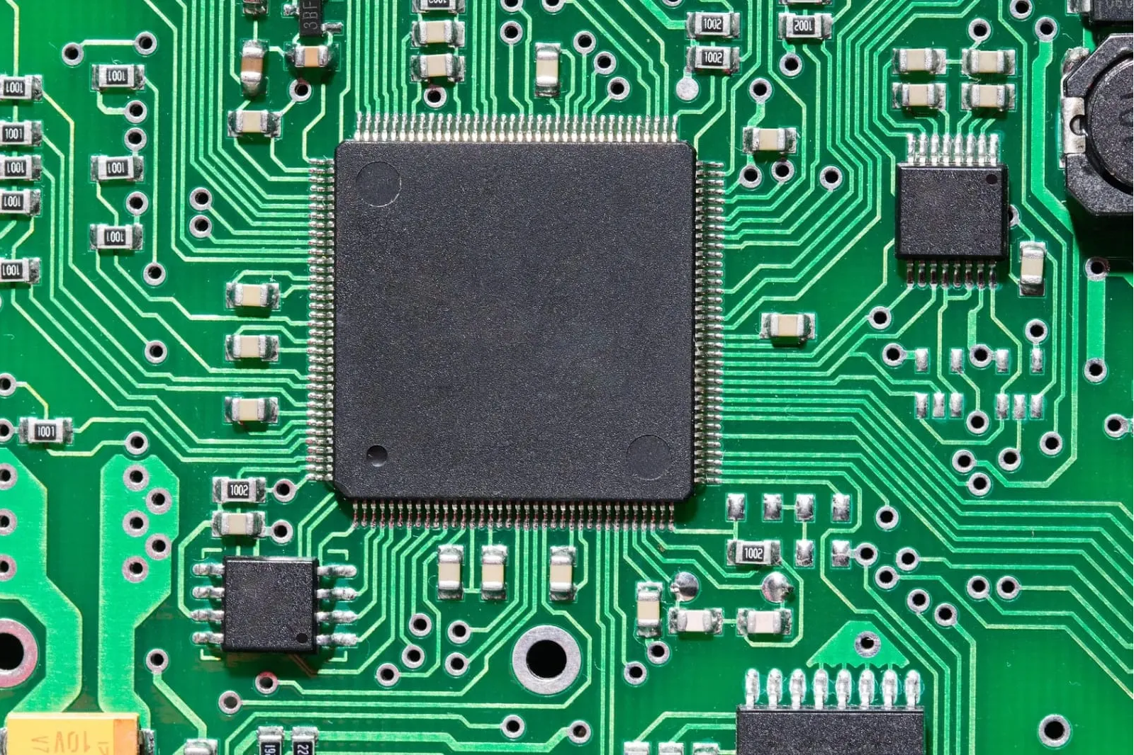
A ground plane is a large area of conductive material, usually copper, on a printed circuit board (PCB) that serves as a common reference point for electrical signals. It acts as the return path for currents, helps stabilize voltage levels, and shields against interference. In essence, a ground plane is like the backbone of your PCB, ensuring that signals travel smoothly without noise or distortion.
In high-speed designs, the ground plane becomes even more critical. It minimizes impedance mismatches and reduces EMI, which can disrupt sensitive components. By providing a low-impedance path for return currents, it keeps your circuit’s performance consistent.
Why Ground Planes Matter for Signal Integrity and EMI Reduction
Signal integrity refers to the quality of an electrical signal as it travels through a circuit. Poor signal integrity can lead to data errors, delays, or complete system failure, especially in high-speed designs. EMI, on the other hand, is unwanted electromagnetic noise that can interfere with nearby components or devices.
A well-designed ground plane tackles both issues. It provides a stable reference for signals, reducing noise and crosstalk between traces. For EMI reduction, the ground plane acts as a shield, absorbing or redirecting stray electromagnetic fields. Without a proper ground plane, return currents might take unpredictable paths, increasing the risk of interference and signal degradation.
For example, in a 4-layer PCB, dedicating an entire layer to the ground plane can reduce loop inductance to as low as 1-2 nH, compared to 10-20 nH with poorly routed return paths. This directly improves signal integrity for frequencies above 100 MHz.
Key Principles of Ground Plane Design
Creating an effective ground plane isn’t just about covering a layer with copper. It requires careful planning to avoid common pitfalls. Let’s explore the core principles of ground plane design.
1. Keep the Ground Plane Continuous
A continuous, unbroken ground plane is ideal for most designs. Breaks or cuts in the ground plane can force return currents to take longer, higher-impedance paths, leading to noise and EMI issues. Aim to cover as much area as possible with a solid ground plane, especially under high-speed signal traces.
2. Understand Signal Return Paths
The signal return path is the route that current takes back to its source through the ground plane. For high-speed signals, the return path should be as short and direct as possible to minimize loop area and inductance. Always route high-speed traces directly above a continuous ground plane to ensure the return current flows beneath the trace, reducing EMI.
For instance, if a signal switches at 500 MHz, even a small deviation in the return path can introduce a delay of 1-2 ns, enough to cause timing errors in critical applications.
3. Avoid Ground Loops
Ground loops occur when there are multiple paths for ground currents to flow, creating unintended voltage differences. These loops can act like antennas, picking up or radiating EMI. To prevent ground loops, use a single-point grounding strategy in low-frequency designs or ensure a solid ground plane in high-frequency designs to eliminate multiple return paths.
Split Ground Planes: When and How to Use Them
Split ground planes involve dividing the ground plane into separate sections, often to isolate analog and digital circuits. While this can reduce noise coupling between different circuit areas, it must be done with caution. Improper splitting can disrupt return paths and worsen EMI.
Use split ground planes only when necessary, such as in mixed-signal designs where analog components are highly sensitive to digital noise. When splitting, connect the planes at a single point (often near the power supply) to maintain a common reference. Additionally, avoid routing high-speed signals over the split, as this can create a large loop area for return currents.
Ground Plane Stitching: Enhancing Performance with Vias
Ground plane stitching refers to the practice of placing vias to connect ground planes across different layers of a multilayer PCB. This technique ensures continuity of the ground plane, especially in areas where traces or components interrupt the plane on a single layer.
Stitching vias reduce the loop area for return currents and help maintain a low-impedance path. They also improve thermal dissipation and mechanical stability. For high-frequency designs operating above 1 GHz, stitching vias spaced at intervals of λ/20 (where λ is the wavelength of the highest frequency) can suppress unwanted resonances.
Best Practices for Via Placement
Via placement is crucial for effective ground plane stitching. Place vias close to high-speed signal transitions or near components with significant ground current. Avoid clustering vias too closely, as this can weaken the PCB structure. A spacing of 0.5 to 1 mm between vias is often sufficient for most designs up to 500 MHz.
Additionally, place vias along the edges of the PCB to create a “via fence,” which helps contain EMI within the board. This is particularly useful for designs that must comply with strict electromagnetic compatibility (EMC) standards.
Practical Tips for EMI Reduction with Ground Planes
Reducing EMI is a top priority for any PCB designer. A well-designed ground plane is your first line of defense. Here are actionable strategies for EMI reduction using ground planes.
1. Use Multiple Ground Planes in Multilayer Boards
In multilayer PCBs, dedicate at least one layer to a solid ground plane. For more complex designs, consider multiple ground planes to provide shielding between signal layers. This approach can reduce crosstalk by up to 20 dB in high-density boards.
2. Minimize Slots and Gaps
Slots or gaps in the ground plane can act as slot antennas, radiating EMI. If a gap is unavoidable (e.g., due to component placement), use stitching vias or small bridges to maintain continuity. Even a 1 mm gap can increase EMI radiation by 10-15% at frequencies above 100 MHz.
3. Decouple Power and Ground Planes
Place decoupling capacitors close to IC power pins to filter out high-frequency noise. Connect these capacitors directly to the ground plane with short, wide traces to minimize inductance. A typical 0.1 μF capacitor can suppress noise up to 100 MHz when placed within 2 mm of the IC.
Common Mistakes in Ground Plane Design
Even experienced designers can make errors in ground plane design. Here are some pitfalls to avoid:
- Routing Signals Over Splits: Never route high-speed signals over a split in the ground plane. This disrupts the return path and increases EMI.
- Insufficient Via Stitching: Failing to use enough stitching vias can create discontinuities, leading to signal integrity issues.
- Ignoring Layer Stackup: In multilayer boards, place ground planes adjacent to signal layers to provide a direct return path. Incorrect stackup can increase crosstalk by 30% or more.
Advanced Considerations for High-Speed Designs
In high-speed PCB designs, such as those for DDR4 memory or USB 3.0, ground plane design becomes even more critical. At frequencies above 1 GHz, small imperfections can lead to significant signal degradation. Here are advanced tips:
- Control Impedance: Match the impedance of signal traces to the ground plane. For a 50-ohm trace, ensure the ground plane is directly beneath with no interruptions.
- Use Differential Pairs: Route differential pairs over a continuous ground plane to maintain symmetry and minimize noise.
- Simulate Return Paths: Use simulation tools to analyze return paths and identify potential EMI hotspots before fabrication.
How Ground Planes Impact Power Integrity
Beyond signal integrity and EMI, ground planes also play a role in power integrity. They help maintain a stable voltage reference for power distribution networks. A solid ground plane reduces voltage drops and ensures that power delivery to components remains consistent, even under high current loads.
For example, in a design with a 3.3V supply and a peak current of 2A, a poorly designed ground plane can cause a voltage drop of 0.1-0.2V due to resistance and inductance. A solid ground plane minimizes this drop to negligible levels.
Conclusion: Mastering Ground Planes for Better PCB Performance
Ground planes are a cornerstone of effective PCB routing. By following best practices in ground plane design, such as maintaining continuity, using ground plane stitching, optimizing via placement, and understanding signal return paths, you can significantly improve signal integrity and achieve EMI reduction. Whether you’re dealing with split ground planes or avoiding ground loops, a thoughtful approach to grounding will elevate the reliability of your designs.
As you work on your next PCB project, prioritize the ground plane from the start. A little extra effort in planning can save hours of troubleshooting later. With these tips, you’re well-equipped to create high-performance, noise-free circuits that meet even the most demanding requirements.
 ALLPCB


