 ALLPCB


Introduction
Differential pairs form the backbone of high-speed signal transmission in modern PCBs, carrying balanced signals for interfaces like USB, PCIe, and Ethernet. These pairs consist of two closely coupled traces that transmit complementary signals, rejecting common-mode noise and preserving data integrity. Yet, routing imperfections often introduce signal integrity issues, such as impedance mismatch and skew problems, which degrade performance at gigabit speeds. Electric engineers frequently encounter these challenges during design validation and prototyping. This practical guide outlines common differential pair troubleshooting techniques and PCB design fixes, drawing on established engineering principles. By addressing root causes systematically, designers can achieve reliable high-speed operation without costly respins.
Understanding Differential Pairs and Their Routing Challenges
Differential pairs operate by sending equal and opposite signals along two traces, where the receiver detects the voltage difference. This configuration provides superior noise immunity compared to single-ended signaling, making it ideal for environments with electromagnetic interference. Routing these pairs requires precise control over geometry, length, and environment to maintain characteristic impedance, typically 90 to 120 ohms differential. Deviations lead to reflections, crosstalk, or timing errors that manifest as bit errors or link failures. In multilayer boards, factors like layer stackup, reference planes, and via transitions amplify these risks. Engineers must prioritize symmetry and consistency from schematic to fabrication.
The relevance of proper routing intensifies with rising data rates, where even minor discrepancies cause eye closure or jitter. Signal integrity issues from poor differential pair routing account for a significant portion of high-speed design failures. Standards like IPC-2221 emphasize guidelines for trace spacing and length matching to mitigate these problems. Understanding the electrical principles behind coupling and propagation delay equips engineers to anticipate issues early. This foundation sets the stage for effective troubleshooting and optimization.
Common Causes of Differential Pair Routing Problems
Impedance Mismatch
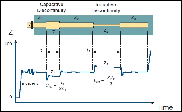
Impedance mismatch occurs when the differential impedance varies along the pair due to inconsistent trace width, spacing, or substrate properties. Variations in copper etching tolerance or dielectric thickness during fabrication exacerbate this, causing signal reflections that distort waveforms. In bends or transitions, abrupt geometry changes further disrupt the controlled impedance profile. Engineers observe this through increased insertion loss or ringing in time-domain reflectometry measurements. Layer stackup asymmetry, such as uneven prepreg distribution, contributes to intra-layer mismatches. Addressing these requires field solver verification during design.
Fab houses report tolerances of plus or minus 10 percent as common, but high-speed designs demand tighter control. IPC-2141 provides methods for calculating and verifying impedance in transmission lines, including differential configurations. Mismatched impedance converts differential signals to common-mode, amplifying EMI susceptibility. Routing over splits in reference planes introduces inductance variations, worsening the mismatch. Proactive stackup planning prevents most occurrences.
Skew Problems
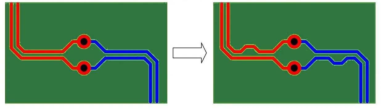
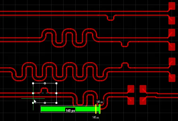
Skew problems arise primarily from length discrepancies within a pair, known as intra-pair skew, or between multiple pairs, termed inter-pair skew. Propagation delay differences, even in picoseconds, desynchronize signals at receivers, leading to setup and hold violations. Serpentine length tuning, if improperly implemented, introduces unwanted coupling or resonance. Unequal via counts or routing paths around obstacles create natural length imbalances. At data rates above 5 Gbps, skew tolerances shrink to below 10 mils, demanding precise matching.
Environmental factors like temperature gradients affect dielectric constant unevenly, dynamically altering skew. Engineers detect this via oscilloscope eye patterns showing reduced height or width. Routing on inner layers with varying effective dielectric constants compounds the issue. Maintaining pair integrity through the entire path, including escape routing, remains critical.
Crosstalk and Coupling Issues
Crosstalk emerges when adjacent differential pairs or single-ended traces couple aggressively due to insufficient spacing. Forward and backward crosstalk degrade noise margins, particularly in dense routing channels. Improper polarity reversal in routing flips the pair, converting balanced signals to odd-mode propagation. Vias placed asymmetrically introduce modal conversion, where differential energy leaks to common-mode.
Reference plane discontinuities force signals into crosstalk-prone regions. Backward crosstalk appears as ghosts on victim traces, mimicking data errors. Spacing rules, typically three times the trace width to adjacent pairs, help contain fields.
Via and Transition Challenges
Vias in differential pairs cause impedance discontinuities from stub capacitance and inductance. Blind or buried vias reduce stub length, but backdrilling adds cost. Asymmetric via pairing shifts the impedance profile, inducing skew. Multiple vias in series compound reflections.
Routing pairs across layer changes requires mirrored via placement and stitching capacitors nearby. These transitions demand simulation to quantify impact.
Troubleshooting Techniques for Differential Pairs
Begin troubleshooting by reviewing the design rules and stackup against simulation results from field solvers. Verify nominal impedance using TDR, targeting flat traces with minimal deviation. Compare measured differential impedance to the target, noting variations at bends or vias. For skew, employ differential TDR or VNA to quantify length differences and phase shifts.
Oscilloscope analysis reveals real-world issues: capture eye diagrams at the receiver, assessing jitter, height, and width. Inject test patterns to isolate deterministic skew from random sources. S-parameter measurements quantify insertion loss, return loss, and crosstalk. Fabricated prototypes benefit from flying probe tests for continuity and basic impedance.
Logical progression involves schematic review first, then layout DRC, pre-layout simulation, post-layout verification, and hardware debug. Correlate failures to specific routing segments.
Practical PCB Design Fixes and Best Practices
Achieving Impedance Control
Select stackup materials with low loss tangents for high frequencies. Route pairs with constant width, gap, and spacing, using 85-mil minimum lengths for field solver accuracy. Employ edge-coupled microstrip or stripline configurations over solid reference planes. Avoid 90-degree bends; use 45-degree or curved transitions. Maintain pair polarity consistently.
For impedance tolerance, specify plus or minus 5 percent in fab notes, aligning with IPC-6012 performance specs for rigid boards. Compensate for etch shrinkage by widening traces slightly.
Minimizing Skew
Implement interactive length tuning with smooth serpentine patterns, limiting amplitude to one-third trace width. Target intra-pair skew below 5 mils for most applications, adjusting per bit rate. Route pairs parallel throughout, avoiding splits. Use same-layer routing where possible to equalize dielectric effects.
Post-route, verify with timing analysis tools extracting actual lengths.
Reducing Crosstalk and EMI
Enforce 3W spacing between pairs and 5H to planes, where W is trace width and H is height. Shield pairs with grounded guard traces if density allows. Route orthogonally to crossing signals.
Optimizing Vias and Transitions
Pair vias symmetrically with equal anti-pad sizes. Use backdrilled through-holes for long stubs. Minimize layer count changes.
Layer and Plane Management
Dedicate inner layers for high-speed pairs over continuous ground planes. Stitch split planes with dense vias. Avoid routing under crystals or switching regulators.
These fixes, applied iteratively, resolve most signal integrity issues.
Real-World Troubleshooting Insights
Consider a multilayer board where PCIe lanes exhibited eye closure post-fabrication. TDR revealed 15-ohm impedance bumps at vias and 20-mil intra-pair skew from unequal routing. Fixes involved rerouting with matched lengths, symmetric blind vias, and impedance tweaks. Post-spin validation confirmed clean eyes. Such cases underscore simulation-layout correlation.
Another scenario involved USB 3.0 pairs with crosstalk from adjacent LVDS. Increasing spacing and adding shielding restored margins. These examples highlight methodical diagnosis.
Conclusion
Troubleshooting differential pair routing demands a structured approach, from impedance mismatch detection to skew correction. By mastering causes like geometry variations and via effects, engineers implement robust PCB design fixes. Adhering to principles in IPC standards ensures repeatability. Proactive verification minimizes respins, enhancing high-speed reliability. Apply these techniques to elevate signal integrity in your designs.
FAQs
Q1: What causes the most common signal integrity issues in differential pair troubleshooting?
A1: Signal integrity issues often stem from impedance mismatch due to inconsistent trace geometry or reference plane splits, alongside skew problems from length imbalances. Crosstalk from tight spacing compounds these at high speeds. Use TDR for diagnosis and symmetric routing for fixes. Maintain tolerances per design requirements.
Q2: How do you fix impedance mismatch in PCB differential pairs?
A2: Verify stackup and trace parameters against field solver models, then adjust width and spacing for target impedance. Route over continuous planes and smooth bends. Reference IPC-2141 for calculation methods. Fabricate with tight etch controls to hold plus or minus 5 percent tolerance.
Q3: What are effective PCB design fixes for skew problems?
A3: Match lengths using serpentine tuning with minimal amplitude, ensuring intra-pair differences stay below critical thresholds. Route symmetrically on uniform layers. Post-layout extraction confirms compliance. This prevents timing errors in high-speed links.
Q4: How can engineers prevent via-related issues in differential pair routing?
A4: Place vias in mirror pairs with equal clearances, preferring blind or backdrilled types. Simulate transitions for reflections. Stitch nearby for return paths. These steps preserve impedance and balance.
References
IPC-2141A — Design and Analysis for Controlled Impedance Transmission Lines Including Differential Pairs. IPC.
IPC-2221 — Generic Standard on Printed Board Design. IPC.
IPC-6012E — Qualification and Performance Specification for Rigid Printed Boards. IPC, 2017


