Introduction
Double-sided printed circuit boards (PCBs) are a cornerstone of modern electronics, offering compact designs with components mounted on both sides. These boards are widely used in consumer devices, industrial equipment, and automotive systems due to their space efficiency. However, their complexity makes troubleshooting and repairing double-sided PCBs a challenging task for electric engineers and electronic hobbyists. Issues such as damaged traces, faulty components, or poor soldering can disrupt functionality. This guide aims to provide a structured approach to identifying faults on double-sided PCBs, mastering soldering techniques for double-sided PCBs, and executing component replacement on double-sided PCBs. By following industry-standard practices, readers will gain practical skills for through-hole repair on double-sided PCBs and ensure reliable outcomes. Let’s explore the essential steps to diagnose and fix these intricate boards effectively.
What Are Double-Sided PCBs and Why Do They Matter
Double-sided PCBs feature conductive copper layers on both the top and bottom surfaces, connected by vias or through-holes. This design allows for higher component density compared to single-sided boards, making them ideal for complex circuits in limited space. They are prevalent in smartphones, power supplies, and medical devices, where efficiency is critical. The importance of repairing double-sided PCBs lies in cost savings and sustainability. Replacing an entire board can be expensive and wasteful, especially in prototype development or small-batch production. For hobbyists, mastering repair techniques extends the life of personal projects. For engineers, it ensures minimal downtime in critical systems. Understanding how to address faults on these boards is a valuable skill in maintaining electronic reliability and performance across industries.
Technical Principles Behind Double-Sided PCB Failures
Understanding the root causes of issues is the first step in troubleshooting double-sided PCBs. These boards are prone to specific failures due to their structure. One common issue is trace damage, often caused by mechanical stress, overheating, or corrosion. Traces on both sides can crack or delaminate, breaking electrical connections. Another frequent problem is via failure, where the plated through-holes lose conductivity due to poor manufacturing or thermal cycling. Component failure, such as capacitors leaking or resistors burning out, also disrupts circuit operation. Soldering defects, like cold joints or bridging, are more challenging on double-sided boards due to limited access. Environmental factors, including humidity and dust, can accelerate wear on exposed areas. Identifying faults on double-sided PCBs requires a systematic approach to pinpoint these issues accurately before attempting repairs.
(Insert image: 'Visual Inspection of Double-Sided PCB' · ALT: 'Close-up view of a double-sided PCB under magnification showing damaged traces')
Practical Steps for Troubleshooting Double-Sided PCBs
Troubleshooting double-sided PCBs involves a blend of visual inspection and electrical testing. Start with a thorough examination under good lighting or magnification. Look for visible signs of damage, such as burnt components, cracked traces, or discolored solder joints on both sides. Pay attention to areas near heat-generating parts, as they are prone to thermal stress. Use a multimeter to check for continuity across traces and vias, ensuring connections are intact. Test for short circuits between adjacent traces, which can occur due to solder bridges. For complex issues, an oscilloscope can help analyze signal integrity at key points. Document findings to track problem areas systematically. This methodical process is essential for identifying faults on double-sided PCBs and sets the foundation for effective repairs.
(Insert image: 'Soldering Double-Sided PCB' · ALT: 'Soldering a component on a double-sided PCB with a fine-tip iron')
Soldering Techniques for Double-Sided PCBs
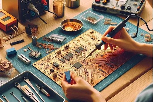
Soldering on double-sided PCBs requires precision due to the presence of components on both sides. Begin by selecting a soldering iron with a fine tip and adjustable temperature control, typically set between 300 to 350 degrees Celsius for most lead-free solders, as per industry guidelines like IPC J-STD-001. Clean the area with isopropyl alcohol to remove contaminants. When desoldering, use a desoldering pump or braid to clear old solder from through-holes without damaging pads. For soldering new components, apply flux to ensure proper wetting and avoid cold joints. Tack down one lead first to secure alignment, then solder the remaining leads. Avoid excessive heat to prevent lifting pads or damaging nearby parts. These soldering techniques for double-sided PCBs ensure reliable connections and minimize rework.
(Insert image: 'Component Replacement Setup' · ALT: 'Removing an SMD component from a double-sided PCB using a hot air station')
Component Replacement on Double-Sided PCBs
Component replacement on double-sided PCBs demands careful handling to avoid damaging the board. Start by identifying the faulty component through testing or visual cues like bulging capacitors or charred resistors. Use a hot air rework station for surface-mount devices (SMDs) to evenly heat and remove the part without stressing adjacent areas. For through-hole components, desolder each lead individually using a pump or wick. Clean the pads thoroughly before installing the replacement. Match the new component’s specifications, such as voltage rating and footprint, to the original. Secure it in place and solder with minimal heat exposure. Verify orientation, especially for polarized parts like diodes. Test the circuit post-replacement to confirm functionality. This process ensures successful component replacement on double-sided PCBs while maintaining board integrity.
(Insert image: 'Through-Hole Repair Process' · ALT: 'Repairing a damaged through-hole on a double-sided PCB with a wire insert')
Through-Hole Repair on Double-Sided PCBs
Through-hole repair on double-sided PCBs is critical when vias or plated holes are damaged, disrupting connectivity between layers. Begin by inspecting the through-hole for cracks or broken plating, often visible under magnification. If the plating is compromised, insert a small wire or a specialized through-hole repair kit to restore conductivity. Solder the wire on both sides, ensuring it does not protrude excessively. Trim excess length for a neat finish. If the pad around the hole is damaged, carefully scrape away the solder mask to expose copper and rebuild the connection with solder. Test continuity with a multimeter to confirm the repair. Adhering to standards like IPC-7721 for repair techniques ensures durability. This approach to through-hole repair on double-sided PCBs restores functionality without replacing the entire board.
Best Practices for Repairing Double-Sided PCBs
Repairing double-sided PCBs requires adherence to best practices to avoid further damage. Always work in a static-free environment using an anti-static wrist strap to protect sensitive components. Organize tools and parts to prevent loss or misplacement during repairs. Use appropriate personal protective equipment, such as safety glasses, when handling soldering equipment. Keep the workspace clean to avoid contaminants affecting solder joints. Document each repair step, especially in professional settings, to maintain traceability. Follow guidelines from standards like IPC-7711/7721 for rework and repair of electronic assemblies. Test the board after each repair stage to catch issues early. These practices ensure that repairing double-sided PCBs is done safely and effectively, extending the board’s operational life.
Common Challenges and How to Overcome Them
Repairing double-sided PCBs presents unique challenges due to their dual-layer design. Accessing components on the bottom side can be difficult if the top side is densely populated. Use a PCB holder or vise to secure the board and rotate it as needed. Thermal damage is another concern, as excessive heat can lift pads or warp the board. Mitigate this by using heat sinks or limiting soldering time. Identifying hidden faults, such as internal layer shorts, requires advanced tools like X-ray inspection if available, though a multimeter suffices for most hobbyists. Patience and precision are key to overcoming these obstacles. By addressing each issue methodically, engineers and hobbyists can achieve successful outcomes in troubleshooting and repairing these complex boards.
Conclusion
Troubleshooting and repairing double-sided PCBs is a valuable skill for electric engineers and electronic hobbyists alike. By understanding the causes of failures, mastering soldering techniques for double-sided PCBs, and following systematic approaches to component replacement on double-sided PCBs, individuals can restore functionality to critical electronics. Through-hole repair on double-sided PCBs and identifying faults on double-sided PCBs are equally essential to ensure long-term reliability. Adhering to industry standards and best practices minimizes errors and enhances repair quality. With the right tools and techniques, anyone can tackle these challenges confidently. This guide serves as a foundation to build expertise in maintaining and repairing double-sided PCBs for diverse applications.
FAQs
Q1: What are the first steps in identifying faults on double-sided PCBs?
A1: Identifying faults on double-sided PCBs starts with a visual inspection under magnification to spot burnt components or broken traces on both sides. Use a multimeter to test continuity and check for shorts. Focus on high-stress areas near heat sources. Document findings to track issues systematically. This approach ensures accurate diagnosis before proceeding with repairs.
Q2: What tools are essential for soldering techniques for double-sided PCBs?
A2: For effective soldering techniques for double-sided PCBs, a fine-tip soldering iron with temperature control is crucial. A desoldering pump or braid helps remove old solder. Flux ensures clean joints, while tweezers aid in handling small parts. A multimeter verifies connections post-soldering. These tools support precision work on complex boards.
Q3: How can I ensure successful component replacement on double-sided PCBs?
A3: Successful component replacement on double-sided PCBs requires confirming the faulty part through testing or visual damage signs. Use a hot air station for SMDs or a desoldering pump for through-hole parts. Match the replacement’s specifications and verify orientation. Test the circuit afterward to ensure functionality. Precision and care prevent further board damage.
Q4: What precautions are needed for through-hole repair on double-sided PCBs?
A4: During through-hole repair on double-sided PCBs, protect the board from static using an anti-static strap. Inspect the hole for plating damage and use a wire or repair kit if needed. Solder carefully on both sides to avoid pad lifting. Test continuity post-repair. Following standard repair guidelines ensures a durable fix.
References
IPC J-STD-001H — Requirements for Soldered Electrical and Electronic Assemblies. IPC, 2021.
IPC-7711/7721C — Rework, Modification and Repair of Electronic Assemblies. IPC, 2017.
IPC-A-600K — Acceptability of Printed Boards. IPC, 2020.
 ALLPCB


