 ALLPCB


If you're looking to optimize your PCB design for manufacturability (DFM) while ensuring top-notch performance, via stitching is a critical technique to master. But what exactly is PCB via stitching, and how does it impact ground stitching, signal stitching, via spacing, and reducing EMI (electromagnetic interference)? In short, via stitching involves placing multiple vias strategically across a PCB to connect layers, improve grounding, enhance signal integrity, and minimize interference. This guide dives deep into the best practices for PCB via stitching DFM, offering actionable insights to help you design reliable and efficient boards.
Whether you're an experienced engineer or just starting out, this comprehensive resource will walk you through everything you need to know about via stitching. From understanding its purpose to implementing it effectively in your designs, we've got you covered with detailed explanations and practical tips.
What Is Via Stitching and Why Does It Matter in PCB DFM?
Via stitching is a design technique used in printed circuit boards (PCBs) where multiple vias are placed to connect different layers, typically to tie ground planes together or support signal transitions. These vias act as electrical and thermal pathways, ensuring better connectivity and stability across the board. In the context of Design for Manufacturability (DFM), via stitching plays a vital role in making sure your PCB is not only functional but also easy and cost-effective to produce.
The primary reasons via stitching matters in PCB DFM include:
- Improved Grounding: Stitching vias connect ground planes across layers, reducing ground loops and ensuring a low-impedance path for return currents.
- Signal Integrity: For high-speed signals, stitching helps maintain consistent reference planes, minimizing signal distortion.
- EMI Reduction: Properly placed vias can shield sensitive areas of the board, cutting down on electromagnetic interference.
- Thermal Management: Vias can dissipate heat from high-power components, preventing overheating during operation.
- Manufacturability: Thoughtful via placement ensures the design aligns with manufacturing capabilities, avoiding issues like drill breakage or uneven copper distribution.
Understanding how to apply via stitching effectively can elevate your PCB design from good to great. Let's explore the different types of via stitching and their specific applications.
Types of Via Stitching: Ground Stitching vs. Signal Stitching
Via stitching can be broadly categorized into two main types: ground stitching and signal stitching. Each serves a unique purpose in PCB design, and knowing when to use them is key to optimizing your layout for performance and manufacturability.
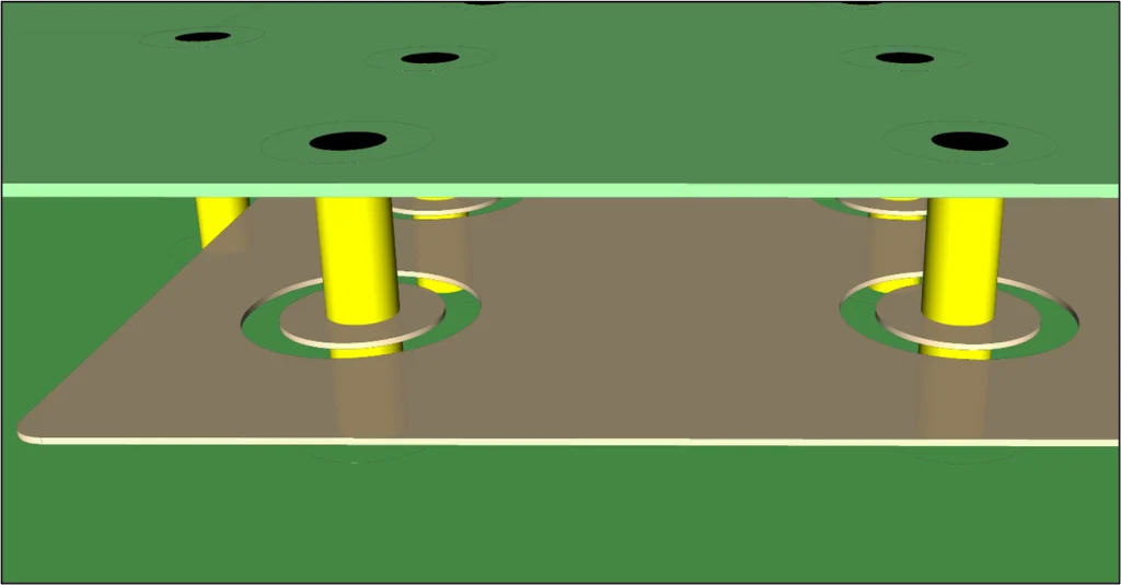
Ground Stitching
Ground stitching involves placing vias to connect ground planes across different layers of a PCB. This technique creates a solid, low-impedance ground path, which is essential for reducing noise and ensuring stable operation in high-frequency or high-current designs.
- Purpose: Minimize ground bounce and provide a consistent return path for currents, which helps in reducing EMI.
- Application: Commonly used around the edges of ground planes or near high-speed components to create a Faraday cage-like effect, shielding against interference.
- Spacing: Vias are often spaced at intervals of about 1/20th of the wavelength of the highest frequency signal on the board (e.g., for a 1 GHz signal, spacing might be around 7.5 mm).
Signal Stitching
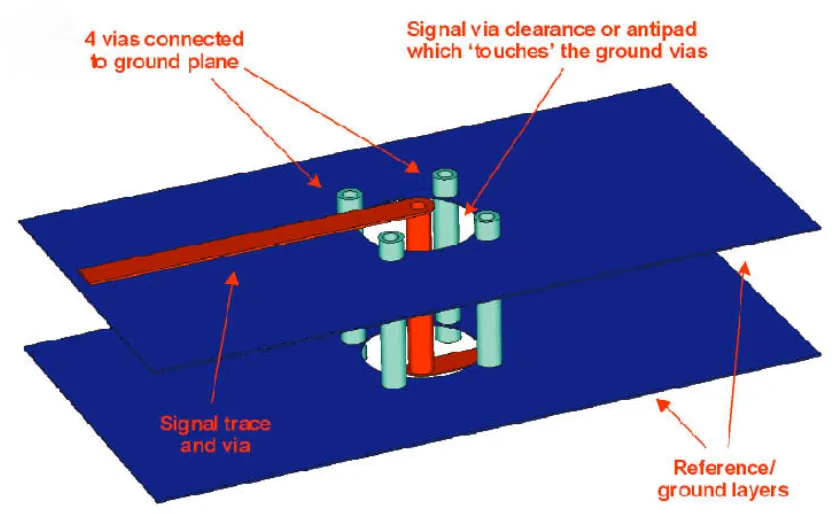
Signal stitching, on the other hand, focuses on maintaining signal integrity by connecting reference planes near high-speed signal traces as they transition between layers. This ensures that the return path for the signal remains uninterrupted, preventing reflections and crosstalk.
- Purpose: Support high-speed signals by providing a nearby reference plane connection, reducing impedance mismatches.
- Application: Used in designs with differential pairs or high-speed digital signals, often placed close to the signal via (e.g., within 0.5 mm for signals operating at 5 Gbps or higher).
- Spacing: Tighter spacing is critical here, often determined by the signal rise time and dielectric properties of the board material.
Both ground and signal stitching are essential for different aspects of PCB performance. However, their implementation must align with DFM principles to avoid manufacturing challenges, which brings us to the importance of via spacing.
Via Spacing: Striking the Right Balance for DFM
Via spacing is a critical factor in PCB via stitching DFM. If vias are placed too close together, they can weaken the board structure, increase manufacturing costs, and cause issues like drill breakage during production. If they’re too far apart, they may fail to provide the necessary electrical or thermal benefits, compromising performance.
Here are some best practices for determining via spacing:
- For Ground Stitching: Space vias based on the frequency of operation. A common rule of thumb is to place vias at intervals less than 1/8th to 1/20th of the wavelength of the highest frequency to prevent resonant cavities that can amplify EMI. For example, at 2.4 GHz (common in Wi-Fi applications), the wavelength is approximately 125 mm, so via spacing should be around 6-15 mm.
- For Signal Stitching: Place stitching vias as close as possible to the signal via, ideally within 0.5-1 mm, to minimize loop inductance and ensure a clean return path. This is especially important for signals with rise times below 1 ns.
- DFM Considerations: Check with your manufacturer for minimum via-to-via spacing rules, often around 0.2-0.3 mm for standard processes, to avoid drilling issues. Overcrowding vias can also lead to uneven copper plating during fabrication.
Balancing via spacing with performance and manufacturability is a delicate task, but it’s crucial for creating a robust PCB design. Next, let’s look at how via stitching helps in reducing EMI, a common challenge in modern electronics.
Reducing EMI with Via Stitching: Best Practices
Electromagnetic interference (EMI) can wreak havoc on PCB performance, causing signal degradation and even regulatory compliance failures. Via stitching is one of the most effective ways to reduce EMI by creating a shielded environment for sensitive signals and ensuring proper grounding.
Here’s how via stitching helps in reducing EMI and some best practices to follow:
- Shielding with Ground Vias: Place stitching vias around the perimeter of ground planes to form a barrier that blocks radiated emissions. This is particularly useful in high-frequency designs where EMI can couple between adjacent circuits.
- Minimizing Ground Loops: By connecting ground planes across layers with stitching vias, you reduce the chances of ground loops, which are a common source of noise and interference.
- Frequency-Specific Spacing: As mentioned earlier, spacing vias at intervals less than 1/20th of the wavelength of the operating frequency prevents resonant cavities that can amplify EMI. For a 5 GHz signal, this translates to a spacing of about 3 mm or less.
- Placement Near Noisy Components: Position stitching vias near components that generate significant noise, such as switching regulators or high-speed processors, to contain interference at the source.
By incorporating these practices into your design, you can significantly cut down on EMI, ensuring your PCB meets performance and compliance standards. However, via stitching for EMI reduction must still adhere to DFM guidelines to avoid overcomplicating the manufacturing process.
Key DFM Considerations for Via Stitching
While via stitching offers numerous benefits, it must be implemented with manufacturability in mind. Ignoring DFM principles can lead to increased production costs, delays, or even design failures. Here are some critical DFM considerations for via stitching:
- Via Size and Type: Use standard via sizes (e.g., 0.3 mm drill diameter) to align with common manufacturing capabilities. Avoid microvias unless absolutely necessary, as they can increase costs and complexity.
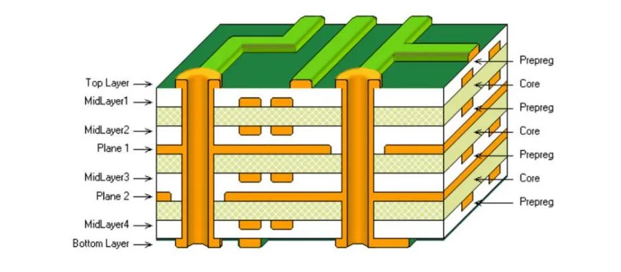
- Layer Stack-Up: Ensure that your via stitching plan matches the layer stack-up of your PCB. For instance, in a 4-layer board, stitching vias might connect the top and bottom ground planes through inner layers, requiring careful planning to avoid signal interference.
- Copper Balance: Excessive via stitching in one area can lead to uneven copper distribution, causing warping during fabrication. Spread vias evenly or consult with your manufacturer to maintain balance.
- Minimum Spacing Rules: Adhere to the manufacturer’s guidelines for via-to-via and via-to-trace spacing to prevent short circuits or drilling issues. Typical minimum spacing might be 0.2 mm for vias and 0.15 mm for traces in standard processes.
- Cost Optimization: While more vias can improve performance, they also increase drilling time and cost. Strike a balance by placing vias only where they’re most needed, such as near high-speed signals or power-hungry components.
By keeping these DFM factors in mind, you can ensure that your via stitching strategy not only enhances performance but also aligns with practical manufacturing constraints.
Common Mistakes to Avoid in Via Stitching
Even with the best intentions, certain pitfalls can undermine the effectiveness of via stitching in your PCB design. Here are some common mistakes to watch out for:
- Overusing Vias: Placing too many vias without justification can complicate manufacturing and increase costs without providing significant benefits. Focus on strategic placement instead.
- Ignoring Signal Return Paths: Failing to place stitching vias near high-speed signal transitions can disrupt return paths, leading to signal integrity issues like crosstalk or reflections.
- Inconsistent Spacing: Uneven via spacing can create weak spots in grounding or shielding, allowing EMI to penetrate or resonate. Stick to calculated spacing based on frequency and design needs.
- Neglecting Manufacturer Guidelines: Not consulting with your fabrication partner about via size, spacing, or count can result in designs that are difficult or impossible to produce reliably.
Avoiding these errors will help you maximize the benefits of via stitching while keeping your design manufacturable and cost-effective.
Tools and Techniques for Effective Via Stitching
Modern PCB design software offers powerful tools to simplify via stitching and ensure it aligns with DFM principles. Here are some techniques and features to leverage:
- Automated Via Stitching: Many design tools allow you to define rules for via placement, such as spacing and grid patterns, to automate the stitching process while adhering to frequency or impedance requirements.
- Simulation and Analysis: Use electromagnetic simulation tools to analyze the impact of via stitching on EMI and signal integrity. This can help you fine-tune spacing and placement before finalizing the design.
- DFM Checks: Run built-in DFM checks in your software to identify potential manufacturing issues related to via size, spacing, or count early in the design process.
By combining these tools with a solid understanding of via stitching principles, you can create designs that are both high-performing and easy to manufacture.
Conclusion: Mastering Via Stitching for PCB DFM
Via stitching is a powerful technique for enhancing the performance and reliability of your PCB designs, especially when it comes to ground stitching, signal stitching, via spacing, and reducing EMI. By following the best practices outlined in this guide, you can ensure that your designs not only meet electrical and thermal requirements but also align with DFM principles for smooth and cost-effective manufacturing.
From calculating optimal via spacing based on operating frequencies to strategically placing vias for EMI shielding, every detail matters. Keep manufacturability in mind by adhering to spacing rules, balancing copper distribution, and consulting with your fabrication partner. With a thoughtful approach to PCB via stitching DFM, you’ll be well on your way to creating boards that excel in both performance and production.
Ready to apply these insights to your next project? Start by reviewing your design for opportunities to implement via stitching effectively, and watch as your PCBs achieve new levels of efficiency and reliability.


