 ALLPCB


If you're looking for a comprehensive PCB life cycle assessment guide, you've come to the right place. Printed Circuit Boards (PCBs) are at the heart of nearly every electronic device, but their production, use, and disposal can have significant environmental impacts. In this ultimate guide, we'll walk you through a full PCB life cycle analysis—from raw material extraction to end-of-life disposal. Whether you're an engineer, designer, or sustainability advocate, you'll find actionable insights on PCB environmental impact analysis and sustainability metrics to make informed decisions.
What Is PCB Life Cycle Analysis (LCA)?
PCB Life Cycle Analysis (LCA) is a method used to evaluate the environmental impacts of a printed circuit board throughout its entire lifespan. This process, often called "cradle to grave" analysis, covers every stage: raw material extraction, manufacturing, assembly, use, and disposal or recycling. By conducting a comprehensive PCB LCA, manufacturers and designers can identify areas to reduce energy consumption, minimize waste, and lower their carbon footprint.
In the sections below, we'll break down each stage of the PCB life cycle, highlight key sustainability metrics, and provide practical tips for reducing environmental impact. Let’s dive into the details of this full PCB life cycle analysis.
Why PCB Life Cycle Assessment Matters
The electronics industry is growing rapidly, with millions of devices produced each year. PCBs are central to this growth, but their production often involves hazardous materials, high energy use, and complex waste management challenges. A PCB environmental impact analysis helps uncover hidden costs, such as pollution from chemical etching or emissions from energy-intensive processes. By understanding these impacts, companies can adopt greener practices and meet regulatory requirements while appealing to environmentally conscious consumers.
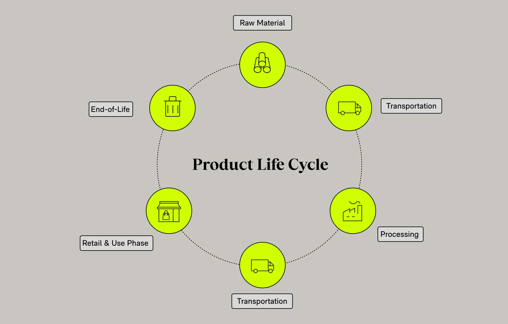
Stages of a Full PCB Life Cycle Analysis
A comprehensive PCB LCA is divided into several key stages. Each stage contributes to the overall environmental footprint, and understanding them is essential for effective sustainability planning. Let’s explore each one in detail.
1. Raw Material Extraction
The life cycle of a PCB begins with the extraction of raw materials like copper, fiberglass, epoxy resin, and precious metals such as gold and silver. Mining these materials can lead to significant environmental issues, including habitat destruction, water pollution, and high energy consumption. For example, producing 1 kilogram of copper can emit around 3.5 kilograms of CO2, depending on the mining process and energy source.
To reduce impact at this stage, consider sourcing materials from suppliers who prioritize sustainable mining practices or use recycled metals. This can lower the carbon footprint before the PCB even reaches the manufacturing stage.
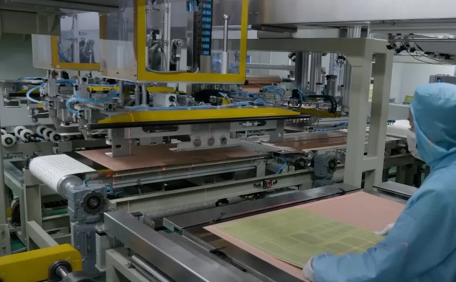
2. PCB Manufacturing and Fabrication
The manufacturing stage is often the most resource-intensive part of a PCB’s life cycle. It involves processes like laminating, drilling, etching, and plating, which require significant amounts of water, chemicals, and electricity. Studies have shown that manufacturing a single square meter of PCB can consume up to 1,500 liters of water and generate hazardous waste, such as copper-laden sludge from etching processes.
One major environmental concern here is freshwater aquatic ecotoxicity potential (FAETP), with up to 89% of this impact attributed to PCB manufacturing, as noted in environmental studies from Turkey. To mitigate this, manufacturers can invest in closed-loop water systems to reduce waste and adopt cleaner chemical alternatives for etching.
3. Assembly and Integration
Once the PCB is fabricated, it moves to the assembly stage, where components like resistors, capacitors, and integrated circuits are soldered onto the board. This process often involves lead-free soldering materials to comply with regulations like RoHS (Restriction of Hazardous Substances). However, soldering still consumes energy and can release volatile organic compounds (VOCs) if not managed properly.
Designers can minimize impact by optimizing PCB layouts to reduce material use and improve energy efficiency during assembly. For instance, reducing the number of layers in a PCB design can lower the energy required for production by up to 20%, depending on the complexity of the board.
4. Use Phase
During the use phase, the environmental impact of a PCB is largely tied to the energy consumption of the device it powers. A poorly designed PCB can lead to higher power losses due to impedance mismatches or inefficient signal routing. For example, a PCB with high impedance in power delivery lines might cause a 5-10% increase in energy loss, depending on the load and frequency of operation (typically measured at signal speeds of 1-5 GHz for high-speed designs).
To address this, engineers can focus on designing energy-efficient circuits and selecting components with low power draw. Extending the lifespan of devices also reduces the need for frequent replacements, cutting down on overall environmental impact.
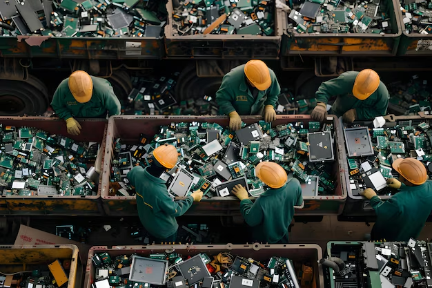
5. End-of-Life: Disposal and Recycling
The final stage of a PCB’s life cycle is disposal or recycling. Unfortunately, many PCBs end up in landfills, where toxic materials like lead or brominated flame retardants can leach into soil and water. It’s estimated that globally, electronic waste (e-waste) generation is around 50 million tons per year, with PCBs making up a significant portion.
Recycling offers a solution, but it’s not without challenges. Recovering valuable metals like gold and copper requires specialized processes that can be energy-intensive. However, recycling a PCB can recover up to 90% of its copper content, reducing the need for new mining. Companies can support sustainability by designing PCBs for easier disassembly and partnering with certified e-waste recyclers.
Key PCB Sustainability Metrics to Track
To conduct a thorough PCB environmental impact analysis, it’s important to measure specific sustainability metrics. These metrics help quantify the environmental footprint and guide improvement efforts. Here are some critical ones to consider:
- Carbon Footprint: Measured in kilograms of CO2 equivalent, this metric tracks greenhouse gas emissions across the PCB life cycle. For instance, manufacturing a single PCB can emit between 10-50 kg of CO2, depending on the energy source and production scale.
- Water Usage: Tracks the volume of water consumed, especially during manufacturing. Reducing water usage by 10% in a mid-sized facility can save thousands of liters annually.
- Energy Consumption: Measured in kilowatt-hours (kWh), this reflects the energy used in production and assembly. Switching to renewable energy sources can cut this metric significantly.
- Waste Generation: Quantifies the amount of hazardous and non-hazardous waste produced. Proper waste management can reduce landfill contributions by up to 30%.
- Recyclability Rate: The percentage of materials that can be recovered at the end of life. Designing for recyclability can boost this rate from 50% to over 80%.
By monitoring these PCB sustainability metrics, companies can set clear goals, such as reducing carbon emissions by 15% over five years, and track progress effectively.
Strategies for Reducing Environmental Impact in PCB Design and Production
Now that we’ve covered the stages and metrics of a full PCB life cycle analysis, let’s look at actionable strategies to minimize environmental impact. These tips are practical for engineers and manufacturers aiming to adopt greener practices.
1. Optimize PCB Design for Efficiency
Start with the design phase. Use simulation tools to optimize signal integrity and power distribution, reducing impedance issues that lead to energy loss. For example, maintaining a controlled impedance of 50 ohms for high-speed signals (common in USB or HDMI interfaces) can improve efficiency by minimizing signal reflection losses, often by 5-10% at frequencies above 1 GHz.
2. Choose Sustainable Materials
Opt for eco-friendly substrates and lead-free solders. Some newer materials, like bio-based resins, can reduce the environmental footprint by up to 20% compared to traditional epoxy resins, based on recent industry studies.
3. Implement Lean Manufacturing
Adopt lean manufacturing principles to cut waste and energy use. For instance, streamlining the etching process to minimize chemical overuse can reduce hazardous waste output by 15-25% in a typical production run.
4. Focus on Circular Economy Principles
Design PCBs with end-of-life in mind. Use modular designs that allow easy component removal for repair or recycling. This approach aligns with circular economy goals and can extend a device’s usable life by years, reducing overall waste.
5. Partner with Responsible Suppliers
Work with suppliers who prioritize sustainability in their operations. This includes sourcing raw materials ethically and ensuring proper waste management practices are in place throughout the supply chain.
Challenges in Conducting a Comprehensive PCB LCA
While a PCB life cycle assessment guide offers valuable insights, there are challenges to conducting a thorough analysis. Data collection can be difficult, especially for small manufacturers who may lack access to detailed supply chain information. Additionally, the diversity of PCB designs and applications means that impact varies widely— a simple single-layer board for a basic remote control has a different footprint than a multi-layer board for a high-end smartwatch.
Despite these challenges, even a streamlined LCA can provide actionable data. Focus on key impact areas like manufacturing and disposal, and use industry benchmarks if specific data is unavailable. Over time, building a robust database of sustainability metrics will make future assessments more accurate.
Conclusion: Building a Sustainable Future with PCB Life Cycle Analysis
A full PCB life cycle analysis is a powerful tool for understanding and reducing the environmental impact of printed circuit boards. From raw material extraction to end-of-life recycling, each stage offers opportunities to improve sustainability through better design, efficient manufacturing, and responsible disposal practices. By tracking PCB sustainability metrics and adopting the strategies outlined in this comprehensive PCB LCA guide, engineers and manufacturers can play a vital role in creating a greener electronics industry.
At ALLPCB, we’re committed to supporting sustainable practices in PCB production. Whether you’re looking to optimize your designs or source eco-friendly materials, our team is here to help you navigate the complexities of PCB environmental impact analysis. Start your journey toward sustainability today by integrating life cycle thinking into your next project.


