When designing a printed circuit board (PCB), the choice of materials plays a crucial role in ensuring the reliability of blind and buried vias. These tiny connections between layers are essential for high-density designs, but their performance can be heavily influenced by the materials used in their construction and plating. So, how do PCB via materials, blind via reliability, buried via reliability, and via plating materials impact the overall durability and functionality of a PCB? In short, the right materials enhance electrical conductivity, thermal stability, and mechanical strength, while poor choices can lead to failures like cracking, delamination, or signal loss.
In this comprehensive guide, we’ll explore the intricate relationship between material selection and via reliability. From the basics of blind and buried vias to the specific impacts of plating and substrate materials, this blog will provide actionable insights for engineers and designers looking to optimize their PCB designs for long-term performance.
What Are Blind and Buried Vias in PCB Design?
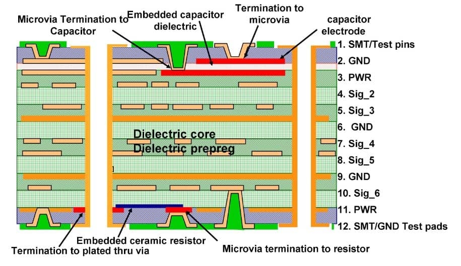
Before diving into the impact of materials, let’s clarify what blind and buried vias are and why they matter in PCB design. Vias are small holes in a PCB that connect different layers, allowing electrical signals to pass through. Unlike standard through-hole vias that go all the way through the board, blind and buried vias are more specialized:
- Blind Vias: These connect an outer layer of the PCB to one or more inner layers but do not go through the entire board. They are visible only on one side, making them ideal for saving space in high-density designs.
- Buried Vias: These are located entirely within the internal layers of the PCB, connecting two or more inner layers without reaching the outer surfaces. They are completely hidden from view and are often used in complex multilayer boards.
Both types of vias are critical in modern electronics, where compact designs and high performance are non-negotiable. However, their reliability depends heavily on the materials used in their construction and the surrounding PCB substrate.
Why Material Selection Matters for Via Reliability
The materials used in a PCB directly affect how well blind and buried vias perform under various conditions, such as temperature changes, mechanical stress, and electrical demands. Poor material choices can lead to issues like via cracking, poor signal integrity, or even complete failure of the board. Let’s break down the key material considerations that impact blind via reliability and buried via reliability.
1. Substrate Materials and Their Role in Via Stability
The substrate, or base material of the PCB, provides the foundation for vias. Common substrate materials include FR-4 (a fiberglass-reinforced epoxy laminate), high-frequency laminates, and polyimide for flexible boards. The choice of substrate impacts via reliability in several ways:
- Thermal Expansion: Materials with different coefficients of thermal expansion (CTE) can cause stress during temperature changes. For instance, FR-4 has a CTE of about 14-17 ppm/°C in the X-Y direction. If the via plating or surrounding materials expand at a different rate, it can lead to cracks or delamination in blind and buried vias.
- Mechanical Strength: Substrates with low tensile strength may not support vias under mechanical stress, especially in flexible or thin boards. This can result in via barrel cracking, a common failure mode in buried vias.
- Moisture Absorption: Some materials absorb moisture more readily, leading to swelling or degradation over time. This can weaken the bond between the substrate and via plating, reducing reliability.
For high-reliability applications, such as aerospace or automotive electronics, engineers often opt for advanced substrates with lower CTE values (closer to 10 ppm/°C) and better moisture resistance to protect blind and buried vias from environmental stressors.
2. Via Plating Materials and Electrical Performance
The plating material used inside vias is another critical factor for reliability. Vias are typically plated with copper to ensure good electrical conductivity, but the quality and thickness of the plating, as well as additional finishes, can make a big difference in performance. Let’s explore how via plating materials affect reliability:
- Copper Thickness: The thickness of copper plating inside vias directly impacts their current-carrying capacity and resistance. For example, a typical via plating thickness is around 1 mil (25.4 micrometers). If the plating is too thin, it can overheat under high current loads, leading to failures. Conversely, overly thick plating can cause manufacturing issues like uneven deposition.
- Plating Uniformity: Uneven copper plating in blind or buried vias can create weak spots, increasing the risk of cracking or poor signal transmission. Advanced electroplating techniques are often used to ensure uniform coverage, especially in deep blind vias.
- Finishes and Coatings: Additional coatings, such as gold or nickel, are sometimes applied over copper to prevent oxidation and improve solderability. However, improper application of these finishes can introduce stress or contamination, reducing blind via reliability.
3. Dielectric Materials and Signal Integrity
The dielectric material between PCB layers insulates the vias and affects signal integrity, especially in high-speed designs. The dielectric constant (Dk) and dissipation factor (Df) of the material play a significant role in how signals travel through blind and buried vias:
- Dielectric Constant (Dk): A lower Dk value (e.g., 3.0-3.5 for high-frequency materials compared to 4.5 for standard FR-4) reduces signal delay and crosstalk in vias, improving performance in high-speed applications.
- Dissipation Factor (Df): A high Df means more signal loss as energy is dissipated as heat. For instance, a Df of 0.02 in standard materials can cause noticeable signal degradation at frequencies above 1 GHz, impacting buried via reliability in multilayer boards.
Choosing the right dielectric material is essential for maintaining signal integrity and preventing issues like impedance mismatches, which can degrade the performance of blind and buried vias.
Challenges in Ensuring Blind and Buried Via Reliability
While material selection is a foundational aspect of via reliability, there are inherent challenges in designing and manufacturing blind and buried vias that must be addressed. These challenges often amplify the importance of using high-quality PCB via materials.
1. Manufacturing Precision for Blind Vias
Blind vias require precise drilling and plating to ensure they connect only to the intended layers. Laser drilling is commonly used for creating small-diameter blind vias (down to 0.1 mm or 4 mils), but inconsistencies in material properties can lead to uneven drilling or plating defects. For example, if the substrate material has uneven resin distribution, it can cause micro-cracks during drilling, compromising blind via reliability.
2. Thermal Stress in Buried Vias
Buried vias, being entirely internal, are particularly vulnerable to thermal stress during manufacturing processes like lamination and reflow soldering. If the CTE of the substrate and via plating materials are mismatched, thermal cycling can cause barrel fatigue or cracking. Studies show that thermal cycling between -40°C and 125°C can reduce via lifespan by up to 30% if materials are not carefully matched.
3. Cost vs. Reliability Trade-Offs
High-performance materials, such as low-CTE laminates or advanced dielectric composites, often come with a higher cost. Engineers must balance the need for reliability with budget constraints, especially in consumer electronics where margins are tight. This trade-off can sometimes lead to compromises in material quality, affecting long-term buried via reliability.
Best Practices for Optimizing Via Reliability Through Materials
To maximize the reliability of blind and buried vias, engineers can follow these best practices when selecting and working with materials:
- Match CTE Values: Choose substrate and plating materials with similar CTE values to minimize stress during thermal cycling. For instance, pairing a low-CTE substrate (around 10-12 ppm/°C) with copper plating can significantly reduce the risk of via cracking.
- Use High-Quality Plating: Ensure that copper plating in vias meets industry standards for thickness and uniformity. A minimum plating thickness of 0.8-1.0 mil is often recommended for high-reliability applications.
- Select Appropriate Dielectrics: For high-speed designs, opt for low-Dk and low-Df dielectric materials to maintain signal integrity through vias. Materials with a Dk below 3.5 are ideal for frequencies above 1 GHz.
- Conduct Reliability Testing: Perform thermal cycling, mechanical stress, and moisture resistance tests on PCB prototypes to identify potential material-related weaknesses in blind and buried vias before mass production.
- Work with Trusted Suppliers: Partner with manufacturers who prioritize quality control in material selection and via fabrication processes to avoid defects that could undermine reliability.
Real-World Applications: How Materials Impact Via Performance
The impact of materials on blind via reliability and buried via reliability becomes even clearer when looking at real-world applications. Here are two examples:
- Automotive Electronics: In automotive control units, PCBs are exposed to extreme temperature swings (from -40°C to 85°C) and vibrations. Using a high-performance substrate with a CTE of 10 ppm/°C and robust copper plating can prevent via failures, ensuring reliable operation over the vehicle’s lifespan.
- High-Speed Communications: In 5G infrastructure equipment, signal integrity is paramount. Blind and buried vias in multilayer boards must use low-loss dielectric materials (Df below 0.005) to minimize signal attenuation at frequencies up to 28 GHz.
Conclusion: Building Reliable PCBs with the Right Materials
The reliability of blind and buried vias is a cornerstone of high-performance PCB design, and the choice of materials is a deciding factor in their success. From the substrate and dielectric to the via plating materials, every component must be carefully selected to withstand thermal, mechanical, and electrical stresses. By understanding the impact of PCB via materials on blind via reliability and buried via reliability, engineers can create designs that meet the demands of modern electronics, whether in consumer gadgets, industrial systems, or cutting-edge communications equipment.
At ALLPCB, we are committed to supporting designers with high-quality materials and manufacturing processes to ensure the reliability of every via in your PCB. By prioritizing material compatibility and rigorous testing, you can build boards that stand the test of time and deliver consistent performance in any application.
 ALLPCB


