 ALLPCB


Introduction
In modern high-speed electronics, achieving precise control over multilayer PCB impedance has become essential for maintaining signal integrity. The layer stackup, which defines the arrangement of conductive and dielectric layers, directly influences PCB trace impedance and overall performance. Engineers designing controlled impedance PCBs must consider how stackup choices affect impedance matching, as mismatches lead to signal reflections, distortion, and increased electromagnetic interference. This article explores the critical relationship between layer stackup and impedance control, providing structured insights for optimizing multilayer designs. By understanding these interactions, designers can enhance reliability in applications ranging from telecommunications to computing systems. Key factors such as dielectric properties and layer sequencing will be examined to guide practical implementation.
Understanding Layer Stackup and Impedance Control
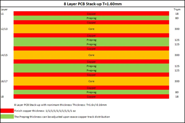
Layer stackup refers to the specific sequence and thickness of materials in a multilayer PCB, including copper foils, cores, and prepregs that form the dielectric separations. In controlled impedance PCBs, the characteristic impedance of traces is determined by the inductance and capacitance per unit length, governed primarily by the geometry and materials surrounding the conductor. PCB layer stack impedance becomes particularly complex in multilayers, where signal traces interact with adjacent reference planes, either as microstrips on outer layers or striplines embedded between planes. Impedance matching ensures maximum power transfer and minimal reflections, critical for high-frequency signals above 1 GHz. Industry guidelines, such as those in IPC-2221A, emphasize the need for consistent stackup documentation to achieve predictable electrical behavior. Poor stackup planning can result in variations exceeding 10 percent in PCB trace impedance, compromising system performance.
This foundational understanding highlights why stackup optimization is non-negotiable for electric engineers working on dense, high-speed boards. Variations in prepreg thickness or core selection alter the effective dielectric height, directly impacting capacitance and thus impedance. Designers must balance mechanical stability with electrical requirements, as asymmetric stackups may cause warpage while symmetric ones support uniform impedance. Reference planes provide return paths and shielding, but their positioning relative to signal layers dictates field confinement. By prioritizing these elements early, engineers mitigate risks associated with fabrication tolerances.
How Layer Stackup Influences PCB Trace Impedance
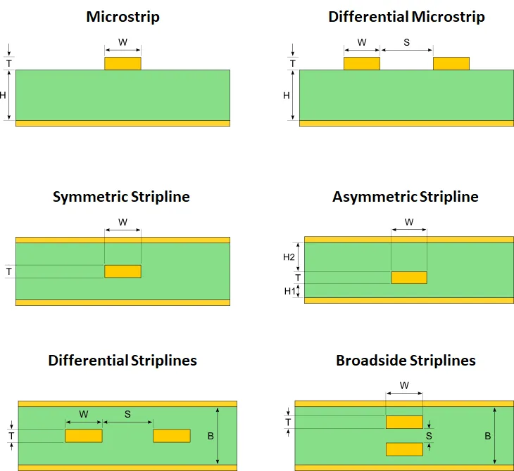
The primary mechanism by which layer stackup affects multilayer PCB impedance is through the control of dielectric thickness between a trace and its nearest reference plane. Thinner dielectrics increase capacitance, lowering impedance, while thicker ones reduce it, raising impedance for a given trace width. Material dielectric constant also plays a role, as higher Dk values further decrease impedance by enhancing capacitive coupling. In practice, outer layer microstrips exhibit higher impedance than inner striplines due to exposure to air, which has a lower effective Dk compared to fully enclosed structures. Engineers must account for these differences when assigning signal layers within the stackup.
Copper thickness and trace width interact with stackup to fine-tune impedance. Heavier copper reduces impedance slightly due to increased conductor volume, but fabrication etching tolerances demand wider traces for consistency. Proximity to power or ground planes minimizes loop inductance, stabilizing PCB layer stack impedance across frequencies. For differential pairs, symmetric stackup ensures balanced fields, crucial for impedance matching in high-speed serial links. Field fringing at edges further complicates calculations, making empirical verification essential.
Routing density influences stackup decisions, as closely spaced traces require tighter dielectric control to avoid crosstalk, which indirectly affects perceived impedance. Plane splits or voids disrupt return currents, causing impedance discontinuities that propagate as reflections. Core and prepreg combinations must match thermal expansion coefficients to prevent delamination, which could alter dielectric spacing post-fabrication. These interactions underscore the need for iterative stackup refinement during design.
Design Principles for Controlled Impedance PCBs
Effective design begins with selecting a stackup that positions signal layers adjacent to continuous reference planes, minimizing dielectric asymmetry. For example, interleaving signal-ground-signal-ground sequences confines fields tightly, achieving stable 50-ohm single-ended or 100-ohm differential PCB trace impedance. Symmetric stackups around the neutral axis reduce warpage, ensuring consistent layer thicknesses critical for impedance repeatability. Designers specify core-prepreg pairings to achieve target dielectric heights, often using multiple thin prepregs for fine adjustments.
IPC-2141A provides guidelines for modeling these structures, recommending field solver validation alongside analytical approximations. Tolerance budgets include etch variation, dielectric constant spread, and copper plating, typically targeting +/- 10 percent impedance control. Outer layers demand wider traces for microstrip compensation, while inner layers allow narrower routing for density. Power plane placement affects decoupling, but excessive distance from signals can elevate impedance through inductive coupling.
- 4-Layer — Signal Layer Position: Outer microstrip, inner stripline — Typical Impedance Structure: 50 ohm single-ended — Key Benefit: Cost-effective for moderate speeds
- 8-Layer — Signal Layer Position: Mixed microstrip/stripline — Typical Impedance Structure: 100 ohm differential pairs — Key Benefit: High density with shielding
- 12-Layer+ — Signal Layer Position: Fully embedded striplines — Typical Impedance Structure: Controlled low-loss paths — Key Benefit: Optimal for GHz+ signals
This list illustrates common configurations, where deeper layers favor lower radiation and tighter impedance control.
Via transitions pose challenges, as stub lengths alter effective impedance; blind or buried vias minimize this in advanced stackups. Material selection favors low-loss dielectrics for high frequencies, though cost constraints often dictate FR-4 hybrids.
Best Practices and Troubleshooting Impedance Issues
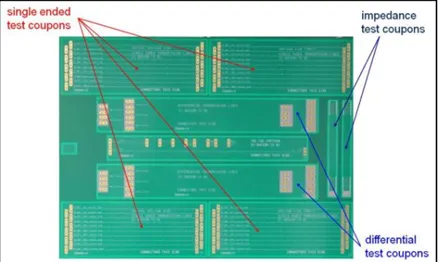
To implement controlled impedance PCB successfully, engineers collaborate with fabricators early, providing detailed stackup drawings with nominal thicknesses and tolerances. Test coupons integrated into panel borders enable time-domain reflectometry measurements, confirming multilayer PCB impedance post-lamination. Adjust trace widths iteratively based on fab data, accounting for resin shrinkage that reduces dielectric height by 10-15 percent.
Common pitfalls include ignoring plane resonance, where large pours create parallel paths altering local impedance. Troubleshooting involves isolating stackup contributions via sectioning and microscopy, correlating with electrical tests. IPC-6012E outlines qualification for rigid boards, ensuring stackup integrity under thermal stress. Maintain via antipad sizes to preserve field distribution without excessive capacitance.
Pre-emphasis on symmetry prevents bow and twist, stabilizing long-term impedance. For high-layer counts, hybrid press cycles control thickness uniformity.
Conclusion
Layer stackup profoundly shapes impedance control in multilayer PCBs, dictating signal quality through dielectric, geometric, and planar interactions. By adhering to principles like plane adjacency and symmetry, engineers achieve reliable PCB trace impedance and matching. Standards such as IPC-2141A and IPC-2221A guide these efforts, bridging design and fabrication. Prioritizing stackup optimization yields robust high-speed boards, minimizing risks in complex systems.
FAQs
Q1: What factors most affect PCB layer stack impedance in multilayers?
A1: Dielectric thickness to reference planes, material dielectric constant, and trace geometry dominate PCB layer stack impedance. Reference plane continuity and copper weight provide secondary influences. Symmetric arrangements ensure uniformity, while fabrication shrinkage demands conservative tolerances. Engineers verify via coupons for production consistency.
Q2: How does stripline differ from microstrip in controlled impedance PCB design?
A2: Striplines, embedded between two planes, offer lower radiation and tighter field confinement for stable multilayer PCB impedance compared to exposed microstrips. Microstrips require wider traces to compensate for air interface effects. Stackup positioning dictates structure choice, balancing density and performance.
Q3: Why is impedance matching critical in high-speed multilayer PCBs?
A3: Impedance matching prevents reflections that degrade signals, ensuring efficient power transfer and low bit error rates. Layer stackup variations amplify mismatches, causing jitter in serial links. Proper PCB trace impedance control via stackup maintains eye diagrams.
Q4: What role do standards play in PCB trace impedance verification?
A4: Standards like IPC-2141A define modeling and tolerance practices for controlled impedance PCB fabrication. They guide test coupon designs and TDR methods for validation. Compliance ensures interoperability across supply chains.
References
IPC-2141A — Design Guide for High-Speed Controlled Impedance. IPC
IPC-2221A — Generic Standard on Printed Board Design. IPC
IPC-6012E — Qualification and Performance Specification for Rigid Printed Boards. IPC


