In the world of PCB design, crosstalk is a common challenge, especially when dealing with high-speed signals. So, how can you minimize the chances of crosstalk on a PCB? The answer lies in strategic component placement and thoughtful layout techniques. By carefully positioning components, spacing traces, and using ground planes, you can significantly reduce interference and ensure signal integrity. In this detailed guide, we’ll dive into the best practices for component placement and other strategies to tackle crosstalk, helping you design reliable and efficient printed circuit boards for high-speed applications.
What Is Crosstalk and Why Does It Matter in PCB Design?
Crosstalk is an unwanted electromagnetic interference that occurs when signals on one trace or component induce noise in a nearby trace or circuit. This phenomenon is particularly problematic in high-speed PCB designs where signals switch at rapid rates, often exceeding 100 MHz. Crosstalk can lead to data errors, timing issues, and overall degradation of circuit performance.
In high-speed designs, the risk of crosstalk increases due to shorter signal rise times and tighter component spacing. For instance, a signal with a rise time of 1 ns can easily couple with adjacent traces if they are too close, causing noise levels that might exceed acceptable thresholds like 100 mV. Understanding and mitigating crosstalk is crucial for maintaining signal integrity, especially in applications like telecommunications, data centers, and automotive electronics.
The Role of Component Placement in Reducing Crosstalk
Strategic component placement is one of the first and most effective steps to minimize crosstalk on a PCB. The physical location of components directly impacts how signals interact with each other. Poor placement can lead to longer trace lengths, increased coupling, and higher chances of interference. Let’s explore how to optimize placement for high-speed signals.
1. Group Related Components Together
Place components that are part of the same signal path close to each other. For example, position a high-speed processor near its memory chips to reduce trace lengths. Shorter traces mean less opportunity for electromagnetic coupling with other signals. As a rule of thumb, aim to keep critical high-speed signal paths under 2 inches if possible, depending on the frequency and board constraints.
2. Separate High-Speed and Low-Speed Circuits
Keep high-speed digital components away from sensitive analog circuits. High-speed signals, such as those from a 500 MHz clock, can easily interfere with low-speed or analog signals if they’re placed too close. Use physical separation to create distinct zones on the PCB for different types of signals. For instance, dedicate one area of the board to digital components and another to analog components to avoid noise coupling.
3. Avoid Placing Sensitive Components Near Noisy Ones
Components like switching regulators or high-frequency oscillators generate significant electromagnetic noise. Place these away from sensitive receivers or amplifiers. If separation isn’t possible due to space constraints, consider adding shielding or ground planes between them to block interference.
Trace Routing Strategies to Minimize Crosstalk
While component placement sets the foundation, how you route traces is equally important in controlling crosstalk on a PCB. Improper routing can undo even the best placement strategies. Here are key techniques to follow when routing high-speed signals.
1. Maintain Adequate Trace Spacing
The closer two traces are, the higher the risk of crosstalk. A general guideline is to maintain a spacing of at least 3 times the trace width (3W rule) between adjacent high-speed signal traces. For example, if your trace width is 5 mils, keep a spacing of 15 mils or more. This reduces capacitive and inductive coupling between traces.
2. Route High-Speed Signals on Different Layers
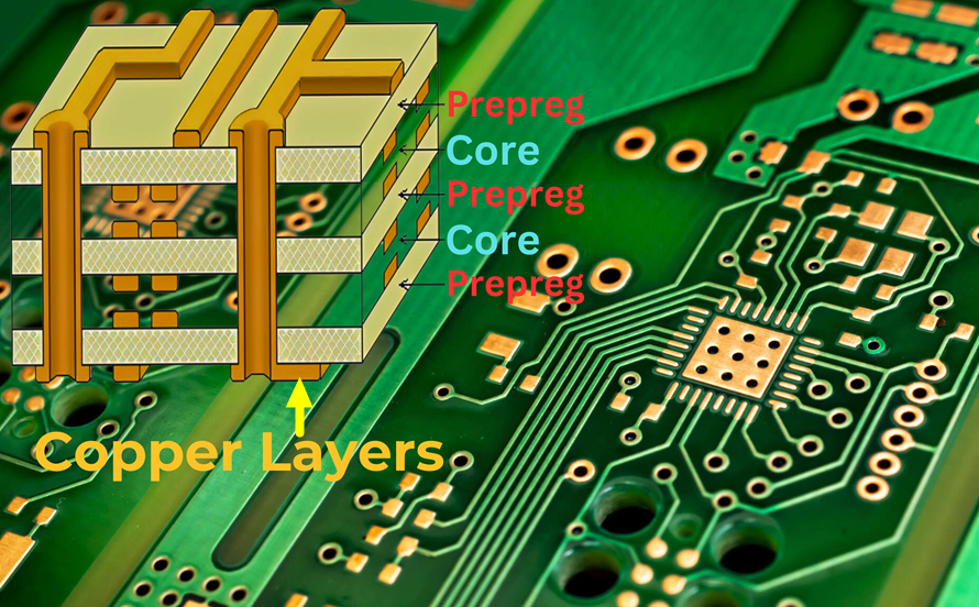
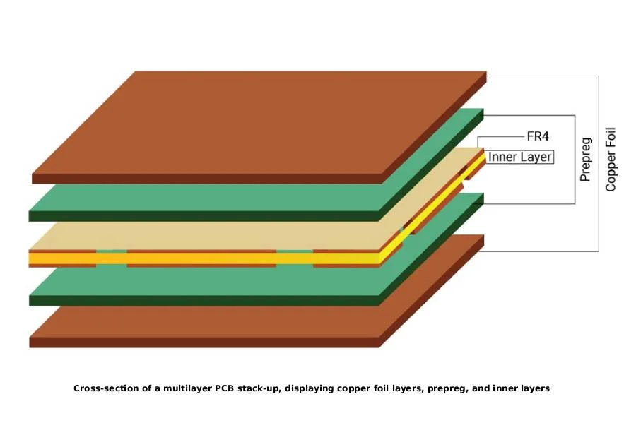
If spacing on a single layer is insufficient, route high-speed signals on different layers of the PCB. Use a ground plane between layers to act as a shield, absorbing stray electromagnetic fields. For instance, in a 4-layer board, route critical signals on the top and bottom layers while sandwiching ground planes in the middle layers.
3. Avoid Parallel Routing Over Long Distances
Running traces parallel to each other for long distances increases the chances of crosstalk due to sustained coupling. If parallel routing is unavoidable, keep the parallel section as short as possible (ideally under 0.5 inches for signals above 200 MHz) and insert a ground trace between them to minimize interference.
Leveraging Ground Planes and Power Integrity
Ground planes are a powerful tool in the fight against crosstalk. They provide a low-impedance path for return currents and act as a barrier to electromagnetic interference. Here’s how to use them effectively in your PCB design.
1. Use Continuous Ground Planes
A solid, unbroken ground plane beneath high-speed signal traces helps to contain electromagnetic fields and reduce crosstalk. Avoid splitting the ground plane unless absolutely necessary, as splits can create high-impedance return paths, worsening interference. For example, a split ground plane might increase noise by 50 mV or more in a high-speed circuit operating at 1 GHz.
2. Place Decoupling Capacitors Strategically
Decoupling capacitors near power pins of high-speed components stabilize the power supply and reduce noise that could contribute to crosstalk. Use capacitors with values like 0.1 μF or 1 μF, placed within 0.1 inches of the power pin, to filter out high-frequency noise effectively.
3. Ensure Proper Return Paths
High-speed signals need a clear return path to minimize loop areas that can radiate noise. Ensure return currents flow directly under the signal trace on the adjacent ground plane. Avoid vias or discontinuities in the return path, as they can increase inductance and lead to crosstalk.
Additional Techniques for High-Speed Signal Integrity
Beyond component placement and routing, other design practices can further minimize crosstalk on a PCB, especially for high-speed signals. Let’s look at some advanced strategies.
1. Use Differential Signaling
Differential signaling, where signals are transmitted as a pair of complementary traces, inherently reduces crosstalk. The noise induced on one trace is canceled out by the opposite noise on the other. This is common in high-speed interfaces like USB or HDMI, where signal speeds exceed 1 Gbps. Route differential pairs close together with consistent spacing, typically 5 to 10 mils apart, to maintain balance.
2. Implement Proper Termination
Signal reflections caused by impedance mismatches can worsen crosstalk. Use proper termination techniques, such as series or parallel resistors, to match the trace impedance (often 50 ohms for high-speed signals). For example, a mismatched 75-ohm trace on a 50-ohm system can reflect up to 20% of the signal energy, increasing noise.
3. Minimize Via Usage in High-Speed Paths
Vias introduce inductance and capacitance, which can disrupt high-speed signals and contribute to crosstalk. If vias are necessary, keep them to a minimum and use back-drilling to remove unused via stubs, which can act as antennas for noise.
Tools and Simulations for Crosstalk Analysis
Modern PCB design software offers tools to simulate and analyze crosstalk before manufacturing. These tools can predict potential interference based on trace geometry, component placement, and signal characteristics. For instance, you can run a crosstalk simulation to identify if a signal trace induces more than 50 mV of noise on a neighboring trace. Use these insights to adjust your layout early in the design process, saving time and cost on revisions.
Additionally, consider following industry standards like IPC-2221 for spacing and routing guidelines. These standards provide tested benchmarks for trace widths, clearances, and other parameters to ensure minimal crosstalk in high-speed designs.
Common Mistakes to Avoid in Component Placement
Even with the best intentions, certain placement errors can increase crosstalk on a PCB. Here are pitfalls to watch out for:
- Overcrowding Components: Packing components too tightly reduces spacing and increases coupling. Always prioritize signal integrity over board size if performance is critical.
- Ignoring Signal Hierarchy: Not prioritizing high-speed signals during placement can lead to longer, more vulnerable traces. Plan your layout with critical paths in mind from the start.
- Neglecting Grounding: Failing to provide adequate grounding near high-speed components can amplify noise. Always ensure a robust ground connection for every IC.
Conclusion: Building Crosstalk-Free PCBs with Strategic Design
Minimizing crosstalk on a PCB starts with strategic component placement and extends to thoughtful routing, grounding, and signal management. By grouping related components, maintaining trace spacing, using ground planes, and adopting advanced techniques like differential signaling, you can significantly reduce interference in high-speed designs. Remember that every detail, from a trace width of 5 mils to a ground plane thickness of 1 oz copper, plays a role in signal integrity.
Designing for high-speed signals doesn’t have to be daunting. With the right approach to component placement and layout, you can build PCBs that perform reliably even at frequencies exceeding 1 GHz. Use the tips and strategies outlined in this guide to create boards that meet the demands of modern electronics, ensuring clear signals and minimal crosstalk every time.
 ALLPCB


