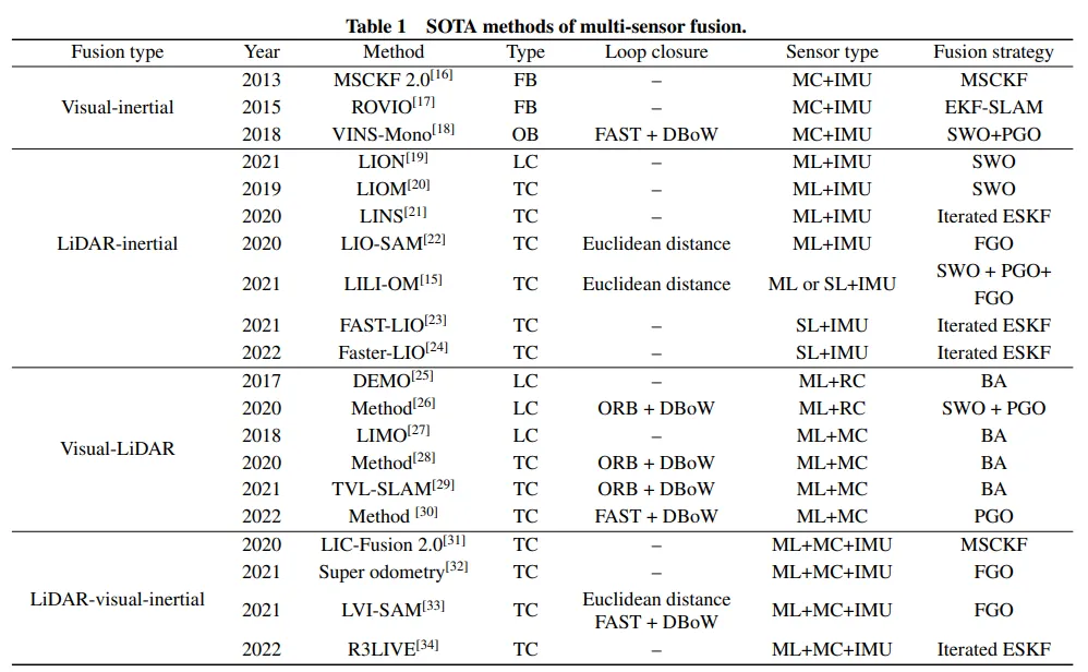
ALLPCB


Overview
Quantum dots (QDs) are semiconductor nanocrystals with tunable sizes in the 1–20 nm range. They exhibit strong light absorption and narrowband emission across the visible and infrared spectra.
Colloidal quantum dots (CQDs) display pronounced quantum confinement effects and can be processed in liquid phase, enabling direct on-chip coupling with silicon-based readout circuits. Infrared imaging devices that integrate infrared detectors for photon absorption and light-emitting diodes for visible-photon excitation can use linear optoelectronic conversion within the device to visualize infrared images directly, avoiding complex readout electronics and signal processing.
Quantum dot properties are adjustable via particle size, material, and composition. Candidate materials include Cd-based, In-based, PbS, perovskites, and emerging materials such as CuInS2, InAs, and ZnTeSe. Different materials yield different bandgaps and thus different absorption and emission spectra.
Under performance comparable to InGaAs sensors, imaging chips based on quantum dots could reduce cost to a small fraction (reported orders of magnitude lower) and potentially enable shortwave infrared (SWIR) imaging in consumer applications.
Historical Milestones
- Photoconductivity was first observed in submarine cable insulation experiments in 1873. The first infrared photoconductive detector was developed in 1917.
- In 1981 and 1983 respectively, Alexei Ekimov and Louis Brus independently identified the quantum size effects of semiconductor nanoparticles.
- The first attempts to use quantum dots in photodetection appeared in 1992, when colloidal quantum dots were explored as photosensitive agents in electronic photography.
- In 1993, Moungi G. Bawendi's group advanced synthesis by thermal injection to produce monodisperse nanoparticles, enabling scalable quantum dot applications.
- Quantum dot infrared photodetectors (QDIPs) were first demonstrated in 1998.
- In 2003, solid-state ligand exchange methods were proposed, facilitating CQD use in optoelectronics.
- In 2005, Edward H. Sargent published on SWIR colloidal quantum dot hybrid photodetectors. Subsequent work, including collaborations between industry and academia, advanced PbS CQD detectors through the 2000s.
- In 2017, a research group demonstrated a graphene/PbS quantum dot transistor-based NIR focal plane array with 388×288 pixels and 35 μm pitch.
- In 2022, a research team reported a PbS quantum dot-based NIR focal plane array and demonstrated imaging under 940 nm illumination.
- Recent advances in quantum dot materials with strong optoelectronic performance have shown potential for integration with silicon-based detectors, offering new approaches to extend silicon sensitivity. Remaining challenges include availability of tailored materials, integration process issues, and the development of matched imaging algorithms.
Current Development Status
Market and Patent Trends
Quantum dot infrared imaging has seen rapid development and expanding application prospects. Patent filings for applying quantum dots to infrared detection rose from around 2005, with early leadership by companies such as InVisage. Filing activity increased markedly around 2011, and while some Western firms reduced filing volume after initial portfolios were established, filings by applicants from China have grown significantly in recent years.
Early patent activity was dominated by foreign applicants, who maintain a lead in terms of earlier filings. Top applicants include mainly foreign entities, while major applicants from China have accelerated their filing activity more recently, particularly around 2022.
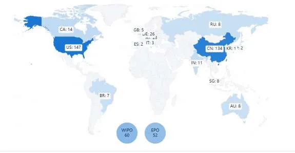
Historically, the US held an absolute advantage in patent filings, with peaks in academic filings around 2011–2012 and increased commercial filings around 2017. Europe saw a filing peak around 2018–2019. Around 2022–2023 the Chinese market's filing volume surpassed others in some datasets; however, many of these filings originate from universities and research institutes rather than companies, indicating that industrialization is still developing.
After family expansion of patent data (publications since 2005), the United States and China emerge as the top target markets, followed by European countries. This reflects both the market size for infrared imaging and the strength of intellectual property protection in those regions, which motivates applicants to file in those jurisdictions.
Technical Classification
Most patents fall under semiconductor and imaging-related IPC classes such as H01L, H04N, G01J, and B82Y. Under H01L, filings have increased for semiconductor devices controlling electrical energy from infrared radiation (H01L31), multiple semiconductor devices on a shared substrate (H01L27), and solid-state devices using organic materials as active components (H01L51). The IPC distribution is similar across regions, with some foreign patents additionally classified under television parts (H04N).
Technology Positioning
Geographic Technology Sources
The United States and Europe are relatively advanced in quantum dot infrared imaging technologies. Analysis of patent family priority data shows that technologies from the US appeared earlier than those from Europe and China, with Europe preceding China.
Patents in the quantum dot infrared imaging field generally exhibit higher value than industry averages, often exceeding typical benchmark levels by factors of 2–6 when compared with related sectors (excluding certain luminescent material categories).
Policy Environment
Since 2015, China has issued a series of policies to promote related industries, and policy activity has been notable in supporting research and industrialization in this area.
Industrial Ecosystem
The upstream of the computer vision and infrared imaging value chain is dominated by a limited number of suppliers, while most companies focus on midstream and downstream activities. In the quantum dot infrared imaging field, many companies concentrate on midstream products such as infrared detectors and imaging modules. Upstream foundational layers are mainly controlled by established global players and include:
- Wafers and auxiliary materials (major foundries and suppliers);
- Quantum dot materials producers (several specialized firms and research suppliers).
Midstream capability is growing in some regions. Traditional infrared imaging companies include established defense and industrial firms, while regional participants from China have increased market share as local capabilities advanced. Academic groups and startups worldwide also contribute to technology development.
Downstream applications split into specialized (defense and subsystem integrators) and civilian markets. Specialized applications include weapon sights, night vision, telescopes, and missile guidance. Civilian applications are diverse, including security surveillance and industrial monitoring. With continued technical progress, infrared imaging costs may decline, enabling wider commercialization and adoption in consumer electronics and other civil markets.
Representative Companies
InVisage
Founded in 2006 in California, InVisage focused on quantum dot-based image sensors and material processes compatible with CMOS fabrication. The company pursued an approach of adding a quantum-dot thin film to standard CMOS processes. InVisage developed an extensive patent portfolio and was acquired by a major technology company in 2017.
ST Microelectronics
ST Microelectronics presented a quantum dot SWIR image sensor expected to be commercializable at the 2021 IEDM conference. The technology is based on PbS quantum dot films integrated into CMOS processes via solution deposition on 300 mm wafers. ST holds several patents covering this approach across multiple jurisdictions.
SWIR Vision Systems
Founded in 2018, SWIR Vision Systems develops CQD image sensors with monolithic integration on CMOS ROICs. Their sensors use PbS CQDs deposited via semiconductor deposition techniques without the need for epitaxial growth or foreign substrates, enabling wafer-scale manufacturing and sub-2 μm pitch p-n photodiode arrays sensitive in SWIR and visible bands. The company has applied its sensors in semiconductor wafer inspection and other industrial uses.
Emberion
Emberion, established in 2016 as a spin-out from an established telecom firm, develops detectors and cameras covering visible to SWIR bands by integrating nanomaterials such as CQDs and graphene on CMOS readout circuits. The company has filed multiple patents in the CQD infrared imaging field.
Qurv Technologies
Qurv Technologies originated from the Institute of Photonic Sciences (ICFO) and develops graphene/quantum dot image sensor platform technology that spans visible to SWIR, aiming for compatibility with low-cost CMOS manufacturing. The company holds a family of patents supporting this platform.