ALLPCB


Wearable electronics continue to drive demand for compact, reliable printed circuit boards that integrate sensors, wireless modules, and power management in small form factors. Engineers developing fitness trackers, medical monitors, and smart textiles require rapid iteration cycles to validate designs before committing to volume production. Quick turn PCB fabrication supports these needs by delivering functional prototypes in days rather than weeks, allowing teams to test mechanical fit, electrical performance, and user comfort early. PCB prototyping services focused on small batches help bridge the gap between schematic capture and final assembly. Design for manufacturability principles applied from the outset reduce the risk of costly revisions later in the process.
Why Quick Turn PCB Fabrication Matters for Wearable Applications
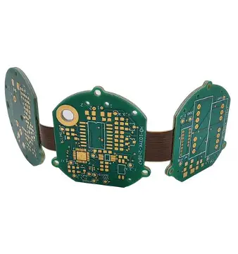
Wearable devices impose strict constraints on board size, thickness, and flexibility that differ from conventional rigid boards. Quick turn PCB fabrication enables designers to evaluate multiple layout iterations within a single development sprint. This speed proves especially valuable when integrating components such as microcontrollers, Bluetooth modules, and flexible interconnects that must survive repeated bending and environmental exposure. PCB prototyping services that accommodate both rigid and flexible substrates allow teams to compare options without long lead times. Early validation through these services improves overall project timelines and reduces the likelihood of discovering manufacturability issues only after tooling investment.
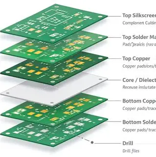
Design for manufacturability becomes critical when boards must fit inside curved housings or conform to body contours. Engineers who incorporate minimum trace widths, adequate spacing, and proper via placement early avoid common fabrication delays. Gerber file generation must accurately represent all layers, including solder mask and silkscreen, to ensure the fabricator can produce boards that match the intended mechanical outline. PCB assembly for prototypes further benefits from clear documentation of component placement and orientation, minimizing errors during hand or automated placement on small runs.
Technical Principles Behind Wearable PCB Prototyping
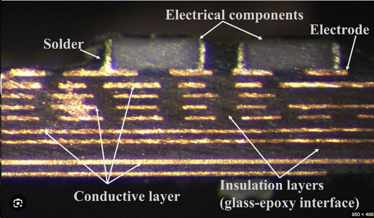
Wearable PCBs often combine rigid sections for component mounting with flexible zones for movement, creating hybrid constructions that require precise control of material properties and lamination processes. Thermal expansion differences between layers can induce stress during reflow, making controlled heating profiles essential. Signal integrity considerations grow important as high-speed data lines for sensors and wireless communication share limited board real estate with power traces. Ground planes and shielding techniques help maintain performance while keeping overall thickness low.
IPC-6012E outlines qualification requirements for rigid printed boards that many quick turn providers follow to ensure consistent quality across prototype batches. Flexible sections typically reference related IPC specifications for bend radius and conductor integrity. These standards emphasize documentation of material properties and process controls that directly affect prototype reliability. Engineers benefit from reviewing fabricator capabilities against these criteria before submitting orders.
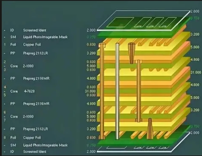
Gerber file generation demands careful attention to aperture definitions and layer alignment to prevent misregistration during imaging. Drill files must specify exact hole sizes and plating requirements, especially for microvias used in high-density wearable layouts. Design rule checks performed prior to file export catch violations that could otherwise cause fabrication holds. Clear stack-up information, including copper weights and dielectric thicknesses, enables the service provider to select appropriate processes for the requested quick turn timeline.
Best Practices for PCB Prototyping Services and Assembly
Successful projects begin with a thorough design for manufacturability review that evaluates panelization options, fiducial placement, and test point accessibility. Engineers should verify that component footprints match available package sizes and that sufficient clearance exists around connectors for assembly tooling. Early collaboration with the prototyping service on material selection helps balance electrical performance, flexibility, and cost for the specific wearable application.
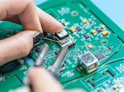
Gerber file generation benefits from standardized naming conventions and inclusion of all required layers in a single zipped archive. A complete readme file describing board thickness, finish type, and any special requirements reduces back-and-forth communication. PCB assembly for prototypes proceeds more smoothly when pick-and-place files and bill of materials are supplied in compatible formats. Stencil design for solder paste application should account for the small pad sizes common in wearables to avoid bridging or insufficient volume.
Quality control steps during quick turn PCB fabrication include electrical testing and visual inspection against acceptance criteria. IPC-A-600K provides visual acceptance guidelines that many providers apply to both rigid and flexible prototypes. Boards destined for wearable use often undergo additional mechanical testing such as flex cycling to simulate real-world conditions. Documentation of these results supports traceability and helps identify process improvements for subsequent iterations.
Conclusion
Quick turn PCB fabrication combined with disciplined design practices accelerates development of wearable electronics while maintaining necessary quality levels. Attention to Gerber file generation, design for manufacturability, and early consideration of PCB assembly for prototypes reduces delays and improves first-pass success rates. Reference to established standards such as IPC-6012E and IPC-A-600K guides consistent evaluation of prototype quality across suppliers. Teams that integrate these elements position their wearable products for reliable performance in demanding end-use environments.
FAQs
Q1: What distinguishes quick turn PCB fabrication from standard production runs?
A1: Quick turn PCB fabrication prioritizes short lead times for small quantities, enabling engineers to obtain functional boards in days for design validation. This approach supports iterative testing of wearable layouts where space constraints and flexibility requirements demand multiple revisions. PCB prototyping services in this category typically maintain dedicated lines for rapid processing while still adhering to relevant IPC specifications for quality.
Q2: How does design for manufacturability improve outcomes in PCB prototyping services?
A2: Design for manufacturability identifies potential fabrication and assembly issues before files are released, reducing the chance of delays or respins. Considerations include trace widths, via placement, and component spacing that align with the capabilities of quick turn providers. Early application of these principles leads to smoother PCB assembly for prototypes and more reliable wearable device performance.
Q3: Why is accurate Gerber file generation important for wearable PCB prototypes?
A3: Accurate Gerber file generation ensures that all layers, drill data, and outlines are correctly interpreted by the fabricator, minimizing errors during quick turn PCB fabrication. Complete documentation supports proper alignment and finish application on compact, often flexible boards. This step directly influences the success of subsequent PCB assembly for prototypes.
Q4: What role does PCB assembly for prototypes play in wearable development?
A4: PCB assembly for prototypes validates component placement, soldering quality, and overall functionality on small batches before scaling. Proper preparation of documentation and adherence to assembly guidelines helps identify issues related to thermal profiles or mechanical stress early. This phase complements quick turn PCB fabrication by confirming that the assembled board meets wearable application requirements.
References
IPC-6012E — Qualification and Performance Specification for Rigid Printed Boards. IPC, 2017
IPC-A-600K — Acceptability of Printed Boards. IPC, 2020
JEDEC J-STD-020E — Moisture/Reflow Sensitivity Classification. JEDEC, 2014