ALLPCB


Are you a hobbyist curious about the environmental impact of your DIY electronics projects? A PCB Life Cycle Analysis (LCA) is a powerful tool to understand how printed circuit boards (PCBs) affect the environment from creation to disposal. In this guide, we’ll walk you through a simple PCB life cycle assessment tailored for beginners, focusing on eco-friendly PCB projects and DIY PCB sustainability. Whether you’re looking to reduce your hobbyist PCB environmental impact or build greener circuits, this step-by-step approach will help you make informed choices.
Let’s dive into the world of PCB LCA for beginners, breaking down each stage of a PCB’s life and offering practical tips to make your projects more sustainable.
What Is PCB Life Cycle Analysis (LCA) and Why Should Hobbyists Care?
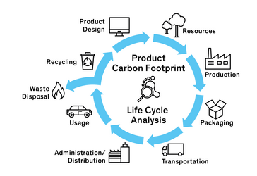
PCB Life Cycle Analysis, or LCA, is a method used to evaluate the environmental impact of a product—in this case, a printed circuit board—across its entire life span. This includes raw material extraction, manufacturing, usage, and end-of-life disposal. For hobbyists, understanding PCB LCA is key to creating eco-friendly PCB projects and minimizing your carbon footprint.
Why does this matter? Electronics, including PCBs, contribute significantly to e-waste, one of the fastest-growing waste streams globally. By conducting a simple PCB life cycle assessment, you can identify ways to reduce waste, conserve resources, and build more sustainable DIY projects. Let’s explore how you can apply LCA to your hobbyist work with a clear, step-by-step process.
Step 1: Understanding the Stages of a PCB’s Life Cycle
Before diving into analysis, it’s important to know the key stages of a PCB’s life. Each stage has unique environmental impacts that hobbyists can influence through thoughtful decisions.
- Raw Material Extraction: This stage involves gathering materials like copper, fiberglass, and epoxy resins to create PCB substrates and conductive layers. Mining and processing these materials consume energy and can release pollutants.
- Manufacturing: PCB production includes etching, drilling, and soldering. These processes use chemicals, water, and electricity, often generating waste and emissions.
- Usage: During use, PCBs are part of electronic devices that consume power. The efficiency of your design affects energy usage over time.
- End-of-Life (Disposal or Recycling): At the end of a PCB’s life, it may end up in a landfill, be incinerated, or be recycled. Improper disposal can release toxic substances into the environment.
Step 2: Assessing Environmental Impact at Each Stage for Hobbyists
Now that you know the stages, let’s look at how to assess the hobbyist PCB environmental impact in each. This is the core of a simple PCB life cycle assessment tailored for beginners.
Raw Material Extraction Impact
The materials used in PCBs, like copper for conductive traces and fiberglass for the substrate, require significant energy to extract and refine. For instance, producing 1 kilogram of copper can emit around 3-5 kg of CO2 equivalent, depending on the mining process. As a hobbyist, you might not mine materials yourself, but choosing suppliers who prioritize sustainable sourcing can reduce this impact.
Tip for Hobbyists: Look for materials labeled as recycled or sustainably sourced when ordering components for your DIY PCB sustainability projects.
Manufacturing Impact
PCB manufacturing often involves chemical etching to remove unwanted copper, which can produce hazardous waste if not managed properly. Energy consumption during production also adds to the carbon footprint. For hobbyists creating boards at home, using less toxic etchants like ferric chloride alternatives or opting for pre-made boards can lower environmental harm.
Tip for Hobbyists: If you etch PCBs at home, use small batches to minimize chemical waste and follow local guidelines for safe disposal.
Usage Impact
During the usage phase, the energy efficiency of your PCB design plays a big role. A poorly designed circuit might draw more power than necessary, increasing its environmental footprint over time. For example, using a microcontroller with a high idle current (say, 50 mA) instead of a low-power one (5 mA) can significantly increase energy use over years of operation.
Tip for Hobbyists: Optimize your designs for low power consumption by selecting energy-efficient components and implementing sleep modes in microcontrollers.
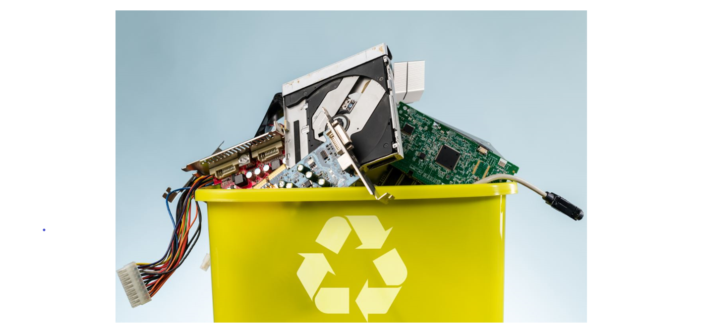
End-of-Life Impact
At the end of a PCB’s life, improper disposal can lead to toxic substances like lead or brominated flame retardants leaching into the environment. Recycling is often the best option, but infrastructure for e-waste recycling isn’t always accessible. Studies suggest that only about 20% of global e-waste is formally recycled, leaving much to harm the environment.
Tip for Hobbyists: Seek out local e-waste recycling programs to dispose of old PCBs responsibly. If possible, salvage components from old boards for reuse in new projects.
Step 3: Tools and Methods for a Simple PCB Life Cycle Assessment
Conducting a full PCB LCA often requires specialized software and data, which might be overkill for hobbyists. However, you can perform a simplified version by focusing on key impact areas and using free online tools or basic calculations.
- Material Inventory: List all materials used in your PCB, including the board substrate, components, and solder. Estimate their environmental impact using general data from sources like environmental reports or databases.
- Energy Use Calculation: Estimate the energy consumed during manufacturing (if you’re making boards at home) and usage. For example, if your soldering iron uses 50 watts and runs for 2 hours per project, that’s 0.1 kWh of electricity per board.
- Waste Assessment: Track the waste generated during manufacturing, such as leftover copper or chemical etchants, and research proper disposal methods to minimize harm.
- Online Calculators: Use free carbon footprint calculators to estimate the impact of your projects based on material and energy inputs.
Tip for Hobbyists: Start with a basic spreadsheet to log materials, energy, and waste for each project. Over time, this data will help you identify patterns and areas for improvement in your eco-friendly PCB projects.
Step 4: Making Your DIY PCB Projects More Sustainable
With your PCB LCA insights, you can take actionable steps to reduce your hobbyist PCB environmental impact. Here are practical ideas for DIY PCB sustainability:
- Use Recyclable Materials: Opt for substrates and components that are easier to recycle. Some newer materials, like bio-based substrates, can reduce global warming potential by up to 39%, according to recent studies.
- Design for Longevity: Build durable circuits that last longer, reducing the need for frequent replacements. For instance, use high-quality components with a rated lifespan of 10,000 hours or more.
- Minimize Waste: Plan your PCB layouts to use the smallest board size possible, reducing material waste. Software tools can help optimize trace routing to fit components efficiently.
- Reuse and Repurpose: Salvage components from old projects or broken devices to use in new builds, cutting down on resource consumption.
- Choose Low-Impact Processes: If you’re etching boards at home, explore less harmful methods like using vinegar-based solutions instead of harsh chemicals.
Step 5: Tracking and Improving Your Environmental Impact Over Time
Sustainability is an ongoing journey. After completing a few projects with PCB LCA in mind, review your data to see where you’ve made progress and where there’s room for improvement. Did switching to low-power components reduce energy use? Did recycling old boards cut down on waste?
Keep a log of each project’s environmental footprint using the simple assessment methods mentioned earlier. Over time, you’ll develop a clearer picture of your hobbyist PCB environmental impact and find new ways to innovate. For example, if you notice that soldering accounts for a large portion of energy use, you might invest in a more efficient soldering station that heats up faster and uses less power.
Benefits of PCB LCA for Hobbyists
Applying a simple PCB life cycle assessment to your projects offers several benefits beyond just environmental impact reduction:
- Cost Savings: Using recycled materials and optimizing designs can lower expenses on components and energy.
- Skill Development: Learning about sustainability pushes you to explore new design techniques and materials, enhancing your electronics skills.
- Community Impact: Sharing your eco-friendly PCB projects can inspire other hobbyists to adopt sustainable practices, creating a ripple effect.
Common Challenges in PCB LCA for Beginners and How to Overcome Them
As a beginner, you might face hurdles when starting with PCB LCA. Here are some common challenges and solutions:
- Lack of Data: Detailed environmental data for specific materials or processes can be hard to find. Use general estimates from online resources or industry reports as a starting point.
- Time Constraints: Conducting an LCA, even a simple one, takes time. Focus on one stage at a time, starting with manufacturing or disposal, to make it manageable.
- Limited Resources: Access to sustainable materials or recycling facilities might be limited. Research local options and connect with online communities for advice on sourcing eco-friendly supplies.
Conclusion: Building a Greener Future with Eco-Friendly PCB Projects
As a hobbyist, you have the power to make a difference through your DIY electronics projects. By following this step-by-step guide to PCB Life Cycle Analysis, you can better understand your hobbyist PCB environmental impact and take meaningful steps toward DIY PCB sustainability. From choosing sustainable materials to optimizing designs and recycling old boards, every small change adds up.
Start with a simple PCB life cycle assessment for your next project. Track your materials, energy use, and waste, then look for ways to improve. Over time, you’ll not only create more eco-friendly PCB projects but also inspire others in the hobbyist community to join the movement for a greener future.
At ALLPCB, we’re committed to supporting hobbyists in their journey toward sustainability. Explore our resources and services to find tools and materials that align with your eco-friendly goals. Together, let’s build circuits that power innovation without harming the planet.