ALLPCB


In the world of printed circuit board (PCB) design, achieving manufacturability while maintaining high performance is a top priority. When it comes to complex designs like High-Density Interconnect (HDI) PCBs, the use of blind and buried vias is essential for saving space and improving functionality. But how do you ensure these vias are designed for efficient production without compromising quality? This guide from ALLPCB dives deep into best practices for designing blind vias, buried vias, and microvias, focusing on manufacturability considerations, aspect ratio, and the plating process.
Whether you're an engineer working on compact electronics or a designer aiming to optimize multilayer boards, this blog will walk you through actionable tips to streamline your PCB design process. Let's explore the key concepts and strategies to make your designs both innovative and production-ready.
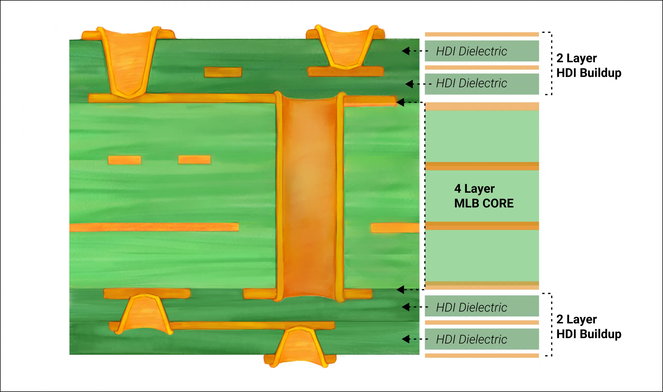
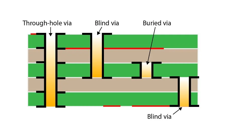
What Are Blind and Buried Vias in PCB Design?
Before diving into best practices, it's important to understand the basics of blind and buried vias, especially in the context of HDI PCBs. These vias are specialized connections that help route signals between layers in multilayer boards without occupying unnecessary space on the surface.
- Blind Vias: These vias connect an outer layer of the PCB to one or more inner layers but do not go through the entire board. For example, a blind via might connect the top layer to layer 2 in a 6-layer board, leaving the bottom layers untouched. This helps save space on the opposite side of the board.
- Buried Vias: These vias are located entirely within the inner layers of the PCB, connecting two or more internal layers without reaching the outer surfaces. For instance, in an 8-layer board, a buried via might connect layers 3 to 5, remaining invisible from the top or bottom.
- Microvias: Often used in HDI PCBs, microvias are smaller in diameter (typically less than 6 mils or 0.15 mm) and are usually laser-drilled. They are commonly used as blind vias to connect closely spaced layers, enabling higher circuit density.
These via types are critical for modern electronics, where devices are shrinking in size while demanding more functionality. However, their design and implementation come with unique challenges that can impact manufacturability. Let's break down the key considerations to ensure your PCB design is production-friendly.
Why Manufacturability Matters in PCB Design with Blind and Buried Vias
Designing a PCB with blind and buried vias without considering manufacturability can lead to production delays, higher costs, and even board failures. Manufacturability refers to how easily and reliably a design can be produced using standard fabrication processes. For HDI PCBs with complex via structures, overlooking this aspect can result in issues like incomplete plating, drilling errors, or thermal stress during assembly.
By focusing on design for manufacturability (DFM), you can minimize these risks. This means aligning your design with the capabilities of fabrication equipment, material properties, and industry standards. For instance, ensuring proper aspect ratios for vias can prevent drilling or plating defects, while selecting the right materials can improve reliability under high-frequency conditions (e.g., signal speeds above 1 GHz).
The goal is to balance innovation with practicality. Let's look at the best practices for designing blind and buried vias to achieve this balance.
Best Practices for Designing Blind and Buried Vias
1. Optimize Via Aspect Ratio for Reliability
The aspect ratio of a via—defined as the ratio of its depth to its diameter—plays a critical role in manufacturability. A high aspect ratio (e.g., 10:1) means a deep, narrow via, which can be difficult to drill and plate properly. For blind vias and microvias in HDI PCBs, maintaining a lower aspect ratio is crucial.
- Recommended Aspect Ratio: For microvias, aim for an aspect ratio of 1:1 or less (e.g., a 4-mil diameter via with a 4-mil depth). For standard blind and buried vias, keep the ratio below 8:1 to ensure consistent plating and avoid voids.
- Why It Matters: A poorly designed aspect ratio can lead to uneven copper deposition during the plating process, causing weak connections or open circuits. This is especially problematic in high-density designs where signal integrity is critical, such as in 5G applications with frequencies up to 28 GHz.
Work closely with your fabrication partner to understand their drilling and plating limits. Adjusting your design to match these capabilities can save time and reduce costs.
2. Understand the Plating Process for Vias
The plating process is a key step in via manufacturing, as it deposits copper inside the via to create a conductive path. For blind and buried vias, achieving uniform plating can be challenging due to their limited accessibility.
- Electroplating Challenges: Blind vias, especially microvias, can trap air or plating solution, leading to voids or insufficient copper thickness. Buried vias, being internal, are even harder to inspect for plating quality.
- Best Practice: Design vias with diameters that allow proper solution flow during plating. For microvias, a minimum diameter of 3 mils (0.076 mm) is often recommended. Additionally, ensure that the via depth does not exceed the fabricator's plating capability—typically around 0.8 times the board thickness for blind vias.
- Thermal Considerations: During assembly, vias undergo thermal stress from soldering (e.g., reflow temperatures up to 260°C). Proper plating ensures the via barrel can withstand this stress without cracking.
By designing with the plating process in mind, you can avoid defects that compromise electrical performance or reliability.
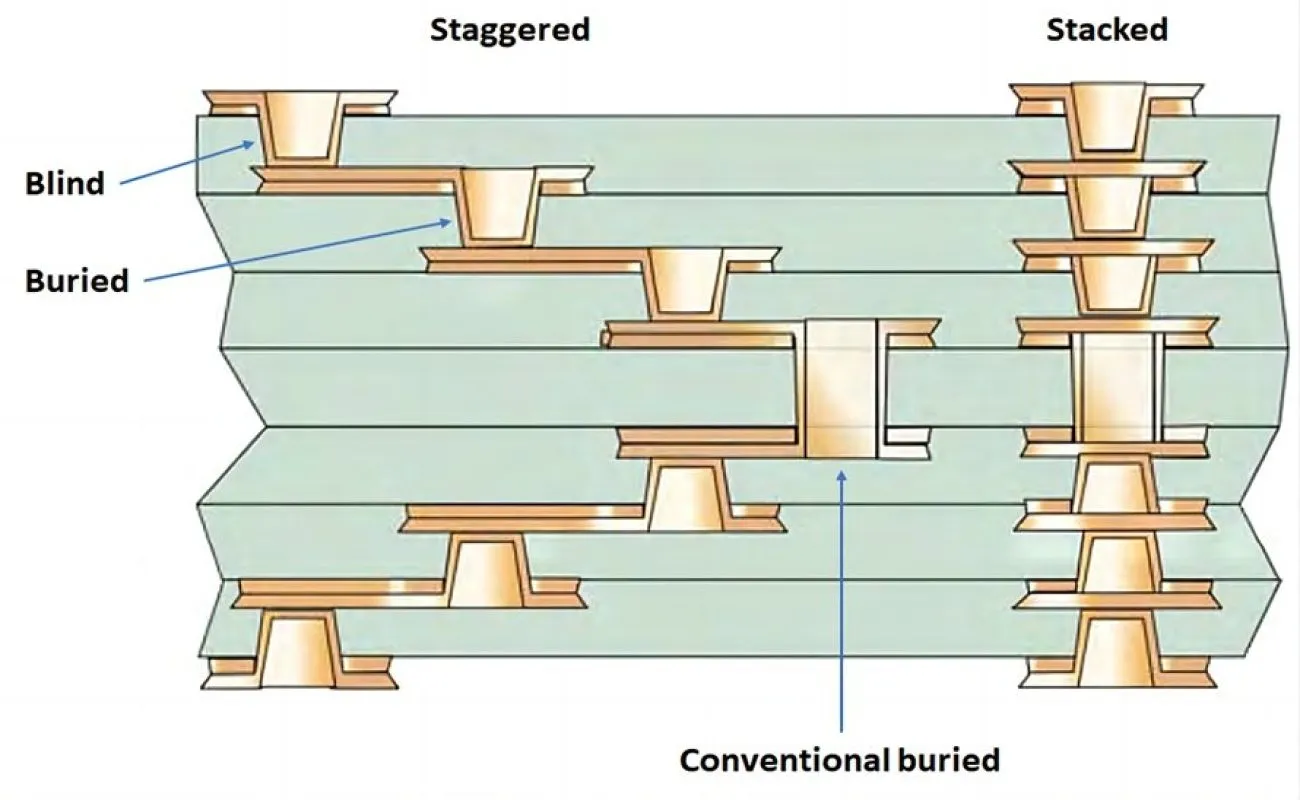
3. Minimize Via Stacking in HDI PCBs
In HDI PCBs, stacking blind vias or microvias on top of each other is a common technique to connect multiple layers in a small area. However, excessive stacking can create manufacturability issues.
- Limit Stacking Depth: Avoid stacking more than two microvias in a single location. For example, stacking a microvia from layer 1 to 2 and another from layer 2 to 3 is generally acceptable, but adding a third via increases the risk of misalignment or structural weakness.
- Impact on Reliability: Stacked vias with high aspect ratios are prone to cracking under thermal cycling, especially in applications with temperature swings from -40°C to 85°C, such as automotive electronics.
If stacking is unavoidable, ensure precise alignment during design and verify the fabricator's capability to handle such structures.
4. Choose the Right Materials for HDI PCBs
The materials used in your PCB design directly impact the manufacturability of blind and buried vias. HDI PCBs often require thin dielectric layers to accommodate microvias, but not all materials are suitable for laser drilling or high-density designs.
- Dielectric Thickness: Use thin dielectrics (e.g., 2-3 mils or 0.05-0.075 mm) for layers connected by microvias. Thicker materials can make laser drilling less precise and increase costs.
- Material Properties: Select materials with low dielectric constants (Dk) and low dissipation factors (Df) for high-frequency applications. For instance, materials with a Dk of 3.0 or lower are ideal for signals above 10 GHz, ensuring minimal signal loss through vias.
Consult with your fabrication team to select materials that balance performance with ease of processing for blind and buried vias.
5. Adhere to Minimum Spacing and Clearance Rules
In high-density designs, spacing between vias, traces, and pads is often tight. However, insufficient clearance can lead to manufacturing defects like short circuits or drilling inaccuracies.
- Via-to-Via Spacing: Maintain a minimum center-to-center spacing of at least 8 mils (0.2 mm) for microvias to prevent overlap during drilling.
- Via-to-Pad Clearance: Ensure a clearance of at least 6 mils (0.15 mm) between vias and adjacent pads to avoid interference during assembly.
Following these spacing guidelines helps ensure that your design can be fabricated without errors, even with tight layouts.
Common Manufacturability Considerations for Blind and Buried Vias
Beyond specific design practices, there are broader manufacturability considerations to keep in mind when working with blind and buried vias in HDI PCBs.
- Fabrication Complexity: Blind and buried vias require sequential lamination, a process where layers are built and bonded step by step. This increases production time and cost compared to through-hole vias. Plan your design to minimize the number of lamination cycles—typically no more than 2-3 for cost efficiency.
- Inspection Challenges: Unlike through-hole vias, blind and buried vias cannot be visually inspected after fabrication. Use X-ray inspection or microsectioning during prototyping to verify via integrity.
- Cost Implications: The use of microvias and complex via structures can raise fabrication costs by 20-30% compared to standard designs. Balance the need for density with budget constraints by optimizing via placement and reducing unnecessary complexity.
Addressing these considerations early in the design phase can prevent costly redesigns and ensure a smoother transition from design to production.
How to Collaborate with Your Fabrication Partner
One of the most effective ways to ensure manufacturability is to collaborate closely with your PCB fabrication partner from the start. Share your design files early and discuss specific requirements for blind vias, buried vias, and microvias.
- Provide Detailed Specifications: Include information on via sizes, aspect ratios, and material preferences in your design documentation.
- Request DFM Feedback: Ask for a design for manufacturability review to identify potential issues before production begins.
- Prototype and Test: Build a small batch of prototypes to test via performance under real-world conditions, such as thermal cycling or high-frequency operation (e.g., signal integrity at 5 GHz).
This partnership approach can help catch issues early and ensure your design aligns with production capabilities.
Conclusion: Designing for Success with Blind and Buried Vias
Designing PCBs with blind and buried vias offers incredible opportunities for creating compact, high-performance electronics, especially in HDI applications. However, success depends on prioritizing manufacturability through careful attention to aspect ratios, plating processes, material selection, and spacing rules. By following the best practices outlined in this guide, you can create designs that not only meet technical requirements but also transition smoothly into production.
At ALLPCB, we're committed to supporting engineers and designers with resources and expertise to bring their ideas to life. Whether you're working on a complex multilayer board or exploring the potential of microvias, these strategies will help you achieve reliable, cost-effective results. Start applying these tips to your next project and see the difference in both design quality and manufacturing efficiency.